


Theory of Operation
Analog Section Detailed Circuit Description
2
2-103
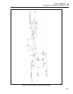
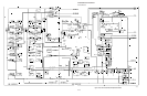
VI+ supplies the output current when sourcing while VI- sinks it. To minimize power
dissipation, the magnitude of the VI± supplies is controlled to minimize the emitter to
collector voltage on the output stage transistors (Q11, Q14). This is done by controlling
the magnitude of the HVCL signal. The controlling function is described later in the
Magnitude Control theory.
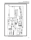
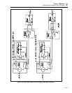
2-163. High Voltage Digital Control
Digital control circuitry on the High Voltage Control assembly (A14) also contains the
control for the High Voltage/High Current assembly (A15). The heart of the digital
control circuitry is an 82C55 Programmable Peripheral Interface IC (U9), which is under
software control via the guarded digital bus. This IC has three ports which generate 24
outputs. These outputs are used to control four 5801 driver ICs (U10-U13), and an
analog multiplexer (U14) for self diagnostics.
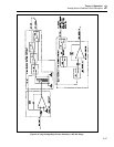
All relays on both HV assemblies are controlled by drivers U10, U11, U12, and U13.
Driver U12 controls relays K14-K16, and generates seven control lines for controlling
various FETs and CMOS Analog Switch ICs contained on both assemblies. Port A
(PA0-PA7) of U9 provides a common input bus for all drivers. Port C (PC0-PC5) of U9
provides the strobe and enable lines for these drivers. Driver U10, which controls the
non-latching relays (K1-K6, K8-K13) on the High Voltage Control assembly, is strobed
by PC1. PC0 is inverted by U8C to provide the enable. Driver U11 controls latching
relay K7 on the High Voltage Control assembly and latching relays K1-K3 on the High
Voltage/High Current assembly. This driver is strobed by PC3. PC2 is inverted by U8D
to provide the enable. Driver U13, which controls the non-latching relays on the High
Voltage/High Current assembly (K4-K12 and K14), is strobed by PC5 and enabled in the
same manner as U10. Driver U12, which generates the Control Lines, is strobed by PC4
and enabled in the same manner as U10. Control line RST, from this driver, is inverted
by U8E to create PS OFF. This control line is used by the magnitude control circuit
described later.
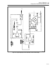
The diagnostic circuit enables the Calibrator to monitor seven points on either the High
Voltage/High Current assembly (A15) or the High Voltage Control assembly (A14). A
4051 analog multiplexer (U14) is controlled by PB4-PB7 of port B of U9. This
multiplexer selects which one of these seven voltages are to be applied to the SDL line
where it is measured by the adc circuit on the DAC assembly (A11). HV MUX0-HV
MUX3 are points on the High Voltage/High Current assembly. HV MUX0 and HV
MUX1 monitor the oven temperature of the H4 and HR7 hybrids respectively. The
output of the dc HV amplifier/ac sense buffer circuit is divided by R18 and R19 to
generate HV MUX2. HV MUX3 monitors the current draw through the HV dc output
series pass circuit to detect an overcurrent condition in the high voltage dc mode.
Resistors R28 and R27 sense the current for a positive high voltage output and a negative
high voltage output respectively. MUX5-MUX7 are points on the High Voltage Control
assembly. MUX5 monitors the high voltage output. HV OUT is divided by R9-R13 and
R64.
This divided output is connected to the output peak measure circuit which uses op amp
U1B. In the dc V function, this circuit is a voltage follower. In the ac voltage function,
this circuit is a peak detector.
The output of U1B charges C5 with R17 being the discharge path. This provides a
positive dc voltage at MUX5. The output of the absolute value circuit is divided by R55
and R56 to generate MUX6. The output of the reference and error amplifier circuit is
divided by R46 and R47 to generate MUX7.