


Theory of Operation
Analog Section Detailed Circuit Description
2
2-75
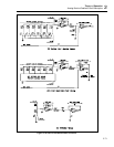
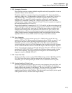
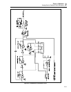
2-123. Averaging Converter
The averaging converter contains the buffer amplifier and rectifying amplifier circuits as
outlined on sheet 1 of the schematic.
The buffer amplifier is a non-inverting unity gain amplifier (U3). Input to the buffer
amplifier is either a 0 or 20 dB attenuator contained in Z2 as selected by K3. In the 2.2V
range, SENSE HI is connected directly to the buffer amplifier with K3 in the reset
position. In the 22V range, K3 is in the set position, so the buffer amplifier input
(SENSE HI) is attenuated 20 dB by the 18 kΩ and 2 kΩ resistors in Z2. The buffer
amplifier output voltage is always between 0.22 and 2.2V, and is capacitively coupled to
the rectifying amplifier by C22 and C25.
The rectifying amplifier is comprised of U5, U7, Q3 and Q4, and has an inverting gain of
2. When the input voltage (from the buffer amp) is positive, feedback is negative through
CR5 and a 2 kΩ resistor in Z1 (pins 6 and 5). When the input voltage is negative, the
feedback path is through CR4 and a different 2 kΩ resistor in Z1 (pins 3 and 5). This
amplifier produces a full-wave rectified negative output current proportional to input
voltage. Output current is summed at the input of the error intergrator with the positive
adjustable reference current (VREF, which is the output of the DAC assembly).
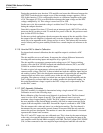
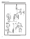
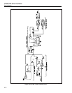
2-124. Error Integrator
The error integrator circuit contains op amp U11, CMOS analog switch U8A, and
capacitors C42 and C43. When operating at frequencies above 119 Hz, op amp U11 and
C43 form an integrator. When operating at frequencies below 119 Hz, control line
LFCOMP* goes low to close U8A, adding C42 to C43. This reduces the integrator
crossover point by a factor of ten. If the magnitude of the averaging converter dc output
current is different than the reference current, the output of the error integrator begins to
change. Error integrator output goes through a three-pole filter and is buffered by U9A to
generate OSC CONT. OSC CONT is routed to the Oscillator Output assembly to adjust
the Oscillator amplitude. The output of the error integrator is also monitored by the
diagnostic circuit via ERROR INT. OUT.
2-125. Three-Pole Filter
The three-pole filter contains op amp U9B, CMOS analog switches U8B-U8D, and C26-
C31. This circuit filters out ac from the output of the error integrator. Control line
LFCOMP* goes low when operating at 119 Hz or less to reduce the crossover point.
2-126. Analog Amplitude Control Loop
This loop is comprised of the averaging converter, error integrator, three-pole filter, and
the agc amplifier on the Oscillator Output assembly (A13). It stabilizes the Calibrator
output voltage in the presence of load changes. This loop by itself is very stable but does
not have the conversion accuracy or gain flatness necessary to meet the precise
amplitude specifications of the Calibrator. Thus this circuit is used only to provide quick
load regulation recovery and short term output stability.