


Theory of Operation
Analog Section Detailed Circuit Description
2
2-73
same as the previous checkpoint. This determines the exact first and second channel
counts for a 0V output.
Next, the +11V and +22V range gain constants are calibrated by nulling the DAC to the
external 10V source, connected to the front panel binding posts of the calibrator. This
10V source is connected to the RCL line by relays on the Switch Matrix assembly (A8).
The RCL line is connected to the +INPUT of the adc amplifier. The DAC output is
connected to the -INPUT of the adc amplifier and is adjusted until the adc reads a null.
This determines the first and second channel counts required for an exact 10 V output
from the DAC. Software determines floating point gain constants from these counts.
The exact value of all the reference voltages (6.5V and 13V) are determined next. The
reference voltage to be determined is connected to the -INPUT of the adc amplifier. The
DAC output is connected to the +INPUT and adjusted until the adc reads a null. The
reference voltage is the value to which the DAC is set. This procedure is done for the
6.5V buffered and unbuffered, and 13V buffered and unbuffered references.
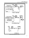
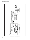
2-118. Oscillator Section Overview
The ac module consists of two plug-in assemblies, the Oscillator Output assembly (A13)
and the Oscillator Control assembly (A12). These assemblies generate a precision
amplitude-stabilized ac sine wave from 0.22V to 22V with a frequency range of 10 Hz to
1.2 MHz. This signal is either routed to the OUTPUT binding posts if the desired output
is within this range, or used internally by the Power Amplifier, High Voltage, Wideband,
Current, Switch Matrix, or an Auxiliary Amplifier (Model 5725A), for voltages and/or
functions outside this range.
Output sensing of the amplitude helps obtain an accurate output signal regardless of
output amplitude and load variations. Sensing is available for all voltage ranges above
200 mV at the calibrator SENSE binding posts. In the current function, and for voltages
less than 200 mV, sensing is performed internally and output accuracy is guaranteed
only for specified operating conditions.
The Oscillator Output assembly (A13) creates an ac voltage. The Oscillator Control
assembly (A12) controls the amplitude of this ac signal by comparing the SENSE HI
signal from the Oscillator Output with an accurate dc voltage from the DAC assembly
(A11). The Oscillator Control assembly adjusts the amplitude of the Oscillator Output
via the OSC CONT line. The frequency accuracy is controlled by the phase-locked loop
circuit on the Oscillator Output assembly, which phase locks to the signal created by the
Current/Hi-Res assembly (A7), or to an external signal connected to the Calibrator rear
panel through the PHASE LOCK IN jack.
The following discussions separately cover these two assemblies.
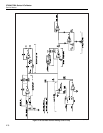
2-119. Oscillator Control Assembly (A12)
The Oscillator Control assembly (A12) contains all the precision ac amplitude control
circuitry except the output AGC amplifier, which is located on the Oscillator Output
assembly (A13). The primary function of the Oscillator Control assembly is to monitor
the output of the Calibrator in the ac voltage function, and to adjust the output until the
rms voltage across the SENSE point is equal to the voltage requested by the operator.
This assembly provides amplitude control for both the ac current function and the
Wideband AC Module (Option -03) during low-frequency operation.
The oscillator control circuitry contains an averaging converter, an error intergrator, a
three-pole filter, an ac/dc thermal transfer circuit, an ac/ac thermal transfer circuit, a 15-
bit dac, and a digital control circuit.