5700A/5720A Series II Calibrator
Service Manual
2-88
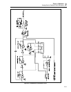
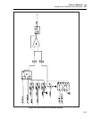
the gate of Q2 is at ground potential. At any frequency, the potential difference between
the gate of Q2 and the base of Q6 results in a current through Q6 as determined by R22,
and by the transconductance of Q2 and Q6. The input stage is called a transconductance
stage because an input voltage results in a current output at the collector of Q6.
This current output is coupled to the mid stage (Q12, Q14, and Q16) by Q8, Q9, Q13 and
C15, where it results in a voltage across the base-emitter of Q16 (the input of the mid
stage). Current source Q9 determines bias current in Q2 and Q6. Variations of Q6 output
current become voltage variations at the base of Q16. This transfer is through Q8 and
Q13 at dc and low frequencies, and through C15 at high frequencies.
The input stage operates with low voltage supplies (±17V) whereas Q16 of the mid stage
is connected to the -PA supply, which can be as high as -365V. This potential difference
is dropped across level shifter Q13.
2-144. PA Mid Stage
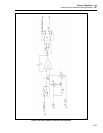
The mid stage (Q12, Q14, and Q16), biased by the 8 mA current source (CR53, Q31,
Q32 and R87 on sheet 2 of the schematic), is a voltage amplifier providing additional
gain. The base of transistor Q16 is the input to the mid stage. MOSFETs Q12 and Q14
are biased by R41 and R53 respectively. Components CR21, CR23, and VR22 protect
Q12 from excessive source-to-gate voltage, and R112 prevents Q12 from oscillating.
Components CR25, CR29, VR28, and R113 perform the same function for Q14. A signal
at the base of Q16 appears amplified at the drain of Q12. Total impedance from the drain
of Q12 to ground, divided by R58, determines gain at dc and low frequencies. At high
frequencies, the effective drain to ground impedance is R53. Relay K12A parallels C18
and C57 during dc operation for a lower bandwidth. Capacitors C18 and C57 provide the
Miller capacitance for the amplifier.
Transconductance gain of the input stage and the Miller capacitance determine Power
Amplifier frequency response at high frequencies. All the voltage gain of the Power
Amplifier comes from the input and mid stages.
2-145. PA Output Stage
The Output Stage is an emitter follower that provides current gain but no voltage gain. It
is needed because the mid stage cannot drive the rated load by itself.
Voltage across R74 and R35 determines the bias current through the output stage. This
voltage equals the voltage across Q7, minus the value (4 x Vbe) (for each transistor Q4,
Q5, Q10, and Q11). Transistor Q7 is configured as a Vbe multiplier, the voltage across
which (and thus the output stage bias current) is the value (1 + (R23+R26)/R32). The
output bias current is 50 mA.
NMOSFETs Q1, Q3, and transistor Q5 source current, while PMOSFETs Q15, Q17, and
transistor Q10 sink current from the load. This output stage can drive up to 50 mA of
load current as determined by the current limit circuit on ±PA supplies on the Filter/PA
Supply assembly (A18).
Zener diodes VR15 and VR18 bootstrap MOSFETs Q3 and Q15 respectively, and
provide the power supplies SC+ and SC- to op amp U1 in the sense current cancellation
circuit. Two stacked NMOSFETs (Q1, Q3) on the top end (+PA side), and two stacked
PMOSFETs (Q15, Q17) on the bottom end (-PA side) withstand the high voltage drops
between ±PA supplies and output. NMOSFETs Q1 and Q3 are biased by R15 and R19
respectively. PMOSFETs Q15 and Q17 are biased by R52 and R57 respectively.
Components CR5, CR7 and VR6 protect Q1 from excessive source-to-gate voltage and
R108 prevents Q1 from oscillating. Protection is also provided for remaining MOSFETs
in the output stage. Output of this stage, called PA OUT HI, is the output of the Power
Amplifier assembly. Components R120 and L10 isolate capacitive loads.


