


Theory of Operation
Analog Section Detailed Circuit Description
2
2-77
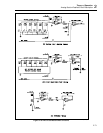
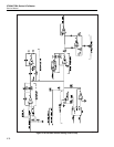
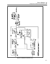
2-127. AC/DC Thermal Transfer Circuit
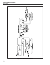
Refer to Figure 2-20 for the following discussion. The ac/dc thermal transfer circuit
achieves basic mid-band amplitude accuracy. This is done by first applying the reference
voltage (VREF) to the thermal rms sensor (U14) and measuring the output. Next, the ac
voltage is applied to the thermal rms sensor and the dc output is compared to the
previous reading. The sensor detects the difference between the ac and dc input voltages
to within a few ppm.
If there is an ac/dc difference, the dc reference current applied to the error integrator of
the analog control loop is adjusted via the 15-bit dac until the ac/dc difference is zero.
The ac/dc thermal transfer circuit that performs this function is further described in
detail. It contains the dc sense buffer, ac sense buffer, ac/dc thermal sensor, and the
square-root amplifier and 15-bit dac as outlined on the schematic.
As previously mentioned, the input to the thermal rms sensor is either the dc reference
voltage (VREF) buffered by the dc sense buffer or the ac voltage (SENSE HI) buffered
by the ac sense buffer.
The dc sense buffer circuit uses op amp U30 as a buffer amplifier. Enhanced-mode FET
Q10 provides feedback for U30 while FETs Q8 and Q9 are off. During a dc transfer,
control line AC*/DC and comparator U21C turn on the FETs, applying the output of the
dc sense buffer to the input of thermal rms sensor U14.
The ac sense buffer circuit contains op amps U12A, U12B, U13; FETs Q6, Q7, Q11,
Q12; relay K4, and associated components. Relay K4 selects the input resistance to
amplifier U13, which has a nominal inverting gain of 0.316 in the 22V range and 3.16 in
the 2.2V range.
During operation in the 22V range, relay K4 is set, feeding the input, SENSE HI,
through the 20 kΩ resistor in Z3. When operating in the 2.2V range, the 2.22 kΩ and
20.0 kΩ resistors in Z3 are put in parallel by K4 in the reset position, reducing the input
resistance to 2 kΩ.
During an ac transfer, control line AC*/DC and comparator U21D turn on FET Q12 so
the output of amplifier U13 is applied to the input of thermal rms sensor U14. At this
time, FET Q11 is turned off and the feedback path for U13 is through the 6.32 kΩ
resistor in Z3.
During a dc transfer, Q12 is off and comparator U21B turns on FET Q11, providing the
feedback path for U13. Op amps U12A and U12B provide low offset and increase the
gain. Control line HFCOMP and comparator U22C turn on FETs Q6 and Q7 during
operation in the 1 MHz range.
The output of either the dc sense buffer or the ac sense buffer becomes the input of
thermal rms sensor U14. During operation from 0.22V to 0.7V in the 2.2V range, or
2.2V to 7V in the 22V range, relay K7 is set, directly connecting the input signal to the
sensor. The input to the thermal sensor is through R31 by K7 in the reset position during
operation from 0.7V to 2.2V in the 2.2V range, or 7V to 22V in the 22V range.
Comparator U21A provides protection for thermal rms sensor U14. If the junction
temperature of the sensor goes above 200ºC, the voltage at pin 3 increases, driving the
output of U21A negative. This turns off the FETs controlling the output of the dc sense
buffer. The ac sense buffer gain goes to zero by turning on FET Q11.