


5700A/5720A Series II Calibrator
Service Manual
2-108
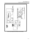
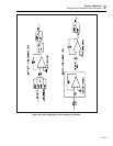
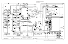
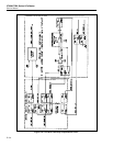
The signal/polarity selection circuit generates the ERROR SIGNAL used by the error
amplifier. It contains op amp U2C, CMOS analog switch U6, and resistor R35-R39.
Control line V/I controls U6B and U6C which select the VI± when in the current mode.
Control lines ±* and ± control U6A and U6D respectively. These switches, operating in
conjunction with U6B and U6C, select between VI±, -SP C or +SP C. In the current
function, U2C subtracts the power supply voltage (VI±) from the absolute voltage
created by the absolute value circuit to create ERROR SIGNAL. This gives a measure of
the emitter to collector voltage of the driving device for each operating function. In the
positive dc voltage function, U2C is configured as a unity-gain inverting op amp. In the
negative dc voltage function, U2C is configured as a voltage follower.
The reference and error amplifier circuit contains op amp U2D, CMOS analog switch
U7B, zener diode VR1, transistors Q2 and Q4, diodes CR10-CR11, capacitor C18, and
resistors R40-R45. Zener diode VR1, R40-R45, Q4, and U7B create a reference voltage.
Control line V/I controls U7B which switches R43-R45 in or out to change this reference
voltage value, depending on the operating function. In the HV dc range, R40 and R41 are
used, balancing the error amplifier with the ERROR SIGNAL near 6.8V. In the 2A dc
range, U7B and Q4 are on, R43 is paralleled with R41, and R45 is paralleled with R40,
so the error amplifier balances when the ERROR SIGNAL is near 3.1V. In the 2A ac
function, Q4 is off, R44 is in series with R45, so the error amplifier balances when the
ERROR SIGNAL is about 5.2V. The output of U2C, ERROR SIGNAL, is summed with
the reference voltage by R40 and R41. This voltage is connected to the error amplifier
U2D which, with C18, is configured as an integrator. The error amplifier generates the
signal AMPLITUDE, which dynamically controls the amplitude of the square wave.
This AMPLITUDE is connected to the input of U7C. -AMPLITUDE, provided by
inverting op amp U1A, is connected to the input of U7D. Control line PS OFF provides a
soft start of the error amplifier. With this line high, Q2 is turned on, shorting C18, which
sets the AMPLITUDE control line to 0V. Once the High Voltage/High Current assembly
is set up for proper operation, this line goes low to turn off Q2.
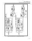
The square wave generator circuit creates a 1 kHz signal QSQB and its complement
QSQB*. These signals are generated by R26, C17, and a stable multivibrator U4.
Control line FREQ controls the CMOS analog switch U7A, which parallels R25 to R26.
This changes the frequency of oscillation to prevent beating when putting out 2A ac near
1 kHz. Control line PS OFF goes high to shut down this oscillator when its not required.
The square-wave amplifier contains op amp U3 and CMOS analog switches U7C and
U7D. Switch U5C is connected to the AMPLITUDE voltage and is controlled by QSQB
from the square wave generator. Switch U7D is connected to AMPLITUDE through
inverting op amp U1A and is controlled by QSQB* from the square wave generator. The
input signal to the square wave amplifier is the output of U7C and U7D. Since QSQB* is
the complement of QSQB, the resulting square wave has a positive peak equal to
AMPLITUDE, and a negative peak equal to -AMPLITUDE. This square wave is
amplified by U3, which is configured for a gain of 2.6, to create HVCL. HVCL is the
square-wave signal used by the Power Amplifier assembly in the previously described
functions.
2-168. Ohms Overview
The Ohms function for the Calibrator is provided by two plug in circuit boards, the
Ohms Main assembly (A10) and the Ohms Cal assembly (A9). These two assemblies
function as one to supply fixed values of resistance from 1Ω to 100 MΩ. Resistance
output is available in values of 1x10
n
(1, 10, 100, 1k ... 100M) and 1.9x10
n
(1.9, 19, 190,
... 19M) from short to 100 MΩ. After the ohms function is calibrated, the Output Display
shows the true value of the resistance selected.