


Theory of Operation
Analog Section Detailed Circuit Description
2
2-79
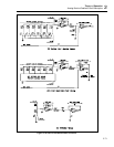
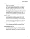
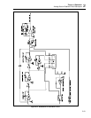
The ac/dc thermal sensor and square-root amplifier, as outlined on the schematic, contain
the thermal sensor U14, op amp U15 and transistor array U17. The dc voltage from the
thermal sensor is connected to U15B configured as an integrator. Comparator U22B is
used to control FETs Q18 and Q20. These FETs are turned on, adding C84 and C62 to
the integrator, by control lines LFCOMP* and AC*/DC both at logic low. The output of
integrator U15B is used by the square-root amplifier contained in U15A, U15C and U17.
This circuit keeps the settling time of the sensor constant when its input is varied
between full and 1/3 scale. The output of the sensor is connected to the RCL line by
relay K6 and CMOS analog switch U19A and U19B. During operation from 0.22V to
0.7V in the 2.2V range, or 2.2V to 7V in the 22V range, sensor output is connected to the
RCL line through buffer U31, U19B, and K6 in the set position. During operation from
0.7V to 2.2V in the 2.2V range, or 7V to 22V in the 22V range, sensor output is
connected to the RCL line through U19A and K6. Control lines SW1 and SW4 control
U19A and U19B respectively. The RCL line is routed to the DAC assembly (A11) where
its amplitude is measured by the adc circuit.
To do an ac/dc transfer, the dc sense buffer is connected to the thermal sensor and the
sensor output is connected to the +input of the DAC’s adc circuit. The -input of the adc
circuit is connected to the DAC output (VREF), and the difference between the two is
measured and stored in memory. Next, the output of the ac sense buffer is connected to
the sensor and the sensor output is connected to the +input of the DAC’s adc circuit. The
difference is measured and compared to the previous reading. The difference between
these two readings is the difference in rms value of the ac and dc input voltages. If there
is an ac/dc difference, the dc reference current applied to the error integrator of the
analog control loop is adjusted via the 15-bit dac until the ac/dc difference is zero.
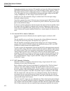
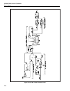
The 15-bit dac contains an AD7534 dac IC (U10), FET Q19 and op amp U26. The first
14 bits (bits 0-13) are generated by the dac IC U10, and bit 14 is generated by Q19, R26,
and control line BIT14. Control busses DATA and MUX from the digital control circuit
select the data and address for U10. The output is inverted by U26 to create 14 BIT DAC
OUT, which is applied to the summing node of the error integrator by R20. This output
is also monitored by the diagnostic circuit.
2-128. Oscillator Calibration
Calibration consists of determining the offset and gain errors of the ac/dc switching
circuitry. Errors are measured at dc using the calibrator DAC and the 6.5V reference as
the primary sources of accuracy. This characterization is valid for frequencies up to 1
kHz. Above 1 kHz, ac/ac characterization is used to ensure the output accuracy.
The DAC assembly (A11) is set to 0V with its output connected to the ac sense buffer
(via SENSE HI) by relay K1 in the set position. The output of the ac sense buffer is
connected to the RCL line by K6 in the set position and by control line GCAL and
comparator U22A turning on Q13. The 0V input is stored as Vin1. The output measured
by the adc circuit on the DAC assembly is stored as Vout1.
Relay K1 ties 6.5V reference BRF6 and BSRF6 to VREF, where it is measured at the
output of the thermal sensor in the same manner as a dc transfer. This measured output is
stored in memory.
The DAC output is set to 20V or 2V and is measured at the output of the thermal sensor
in the same manner as an ac transfer. The DAC is then adjusted until this measured
output is the same as stored in the previous step. The DAC setting is stored as Vin2 and
the 6.5V reference is Vout2. The gain can now be calculated with the formula: (Vout2 -
Vout1)/(Vin2 - Vin1).