5700A/5720A Series II Calibrator
Service Manual
2-30
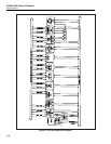
transistors. When AOUT is high, U13B turns Q2 and Q4 on. Q4 turns Q6 on, providing a
path for the filament current through Q2 and Q6. Zener diode VR2 provides the dc
voltage offset necessary for proper filament operation. Then when BOUT is high, U13A
turns Q1 and Q3 on. Q1 turns Q5 on, providing a path for the filament current through
Q3 and Q5, effectively reversing the direction of the voltage driving the filament. Zener
diode VR1 provides the dc voltage offset necessary for proper filament operation.
PLD U4 also generates the 225 Hz square-wave SCAN signal used by PLD U9 to control
front panel keypad scanning and key debounce.
Dual-port RAM U1 contains all the Control Display data written by the 68HC000
microprocessor on the CPU board. PLD U4 contains a 10-bit address counter which is
used by U4 to read the contents of U1. U1 provides a BUSYD signal to U3, which is
active low whenever the CPU and U4 try to access the same RAM location at the same
time. If the microprocessor attempts to write to the RAM location that U4 is reading (as
it refreshes the DMD), U3 uses BUSYD to hold off DTACK to the microprocessor. This
prevents the written data from being lost. The other busy signal, generated when U4
attempts to read from a location being written to by the microprocessor, is ignored.
Losing display data for one refresh cycle is insignificant.
The Control Display can be blanked to maintain its brightness over years of operation.
The Main CPU pulls U10 pin 12 (SQ) low when the Calibrator has been inactive for at
least 30 minutes. This action results in U13 E&F being driven low to short the bases of
Q5 and Q6 to common, turning off any filament drive to the control display. Since U13
outputs are open-collector, they have no effect on the filament drive circuit when the
Main CPU returns U10 pin 12 high.
2-51. Output Display Circuitry
Output display circuitry consists of a custom 2-row, 22-character vacuum-fluorescent
display under the control of PLD U5. The circuit contains high voltage grid driver U15,
high voltage anode driver U14, a filament switching circuit, and a 1K x 8 (1 KB) dual-
port RAM, U2.
The custom display is divided into 24 grids. The 22 characters are made up of fourteen
seven-segment digits and eight 14-segment characters.
IC U5 is an EP900 PLD, programmed to provide the timing and control signals for the
output display circuitry. Display data written by the microprocessor into the Output
Display’s dual-port RAM U2, is read by U5 and sent serially to the high voltage anode
driver. Both the anode and grid drivers are serial TTL-level input, 32-bit parallel high
voltage output devices. Only 31 anode driver outputs and 24 grid driver outputs are used,
the remaining high voltage outputs are left unconnected. IC U5 also controls grid timing
and display refresh.
A special refresh scheme is used by the Output Display to intensify a specific digit to be
displayed. This feature is used by the Calibrator when in Error Mode, while editing a
value displayed on the Output Display. The digit selected for editing is brighter than the
other digits. To accomplish this, U5 monitors data it reads from the dual-port RAM.
Following the entry of the fourth data byte to the input registers of the anode driver, the
registers are strobed to the high voltage output drivers, then the drivers are enabled. If
data bit D7 of the fourth byte is low, the state machine in U5 simply goes on to refresh
the next digit at the normal rate of approximately 200 Hz. If, however, bit D7 of the
fourth byte is high, the state machine enters a delay routine that adds about 625 us to the
normal 5 ms anode and grid on-time, thereby intensifying the digit. Unlike the Control
Display, only one grid at a time is turned on.


