


5700A/5720A Series II Calibrator
Service Manual
2-106
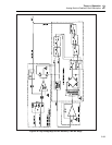
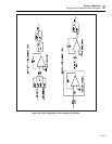
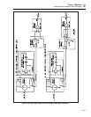
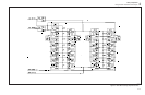
2-166. Calibration of the Current Function.
Refer to Figure 2-29 for the following discussion. The resistor network Z5 determines
the accuracy of the 2.2A current range. Calibration involves determining its offset and
gain constants. The Calibrator is configured as in the 2.2A dc function, except that the
Current assembly (A7) is set to the 2.2 mA range.
To determine offset, the output (B CUR) is routed back to the Current assembly where it
is connected to INT OUT HI. INT OUT HI is routed to the Ohms Main assembly (A10),
where it is connected to a previously calibrated 10Ω resistor. The voltage generated
across this 10Ω resistor is routed to the differential amplifier on the Ohms Cal assembly
(A9). The output of the differential amplifier is routed to the DAC assembly (A11)
where it is measured by its adc circuit. A checkpoint reading is first taken by removing
INT OUT HI from the 10Ω resistor and measuring the voltage across the resistor. The
offset is then measured by connecting INT OUT HI to the 10Ω resistor. The DAC
assembly, which controls the output of the Current assembly, is adjusted until the adc
circuit measures the same as the previous checkpoint reading.
To determine gain, the Calibrator is configured as in the previous step, except with the
Current assembly outputting 1.3 mA generated from the 13V reference (BRF13 and
BSRF13) from the DAC assembly. This 1.3 mA is amplified 100 times by the 2.2A
amplifier. The resulting 130 mA is connected to the 10Ω resistor on the Ohms Main
assembly by the same path as for the offset calibration. The resulting 1.3V across this
10Ω resistor is routed to the Ohms Cal assembly (A9), where it is connected to the -input
of the differential amplifier. The +input of the differential amplifier is connected to the
output of the DAC assembly. The output of the differential amplifier is connected to the
RCL line which is routed to the adc circuit on the DAC assembly. The DAC output,
which is the +input of the differential amplifier, is adjusted until a null is measured on
the RCL line by the DAC’s adc circuit. This step is repeated by changing the -input of
the differential amplifier to the other side of the 10Ω resistor. The software now
computes the exact voltage drop across the 10Ω resistor. Gain is determined by using
this and the previous offset reading.
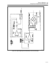
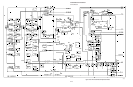
2-167. High Voltage Magnitude Control
The square wave (HVCL) used in the previously described functions, is created and
amplitude controlled by the High Voltage Control assembly (A14). This circuitry, shown
on sheet 2 of the schematic, contains the absolute value circuit, signal/polarity selection
circuit, reference and error amplifier, square wave generator, and the square wave
amplifier.
The absolute value circuit contains op amp U2A, U2B, Q3, diodes CR8 and CR9,
capacitor C20, and resistors R27-R32 and R68. During operation in the ac current
function, this circuit creates an absolute value of the G OUT signal from the collectors of
the 2.2A output transistors. Op amp U2A generates a negative half-wave signal equal to
the positive peaks of G OUT. Resistors R32 and R27 sum this half-wave signal and the
input signal G OUT at the input of U2B. Capacitor C20 averages the voltage so the
output of U2B is a dc voltage which represents the positive peak voltage of G OUT. In
the high voltage dc function, the 2.2A amplifier circuit is not used, so the output of U2B
is 0V.