


Theory of Operation
Analog Section Detailed Circuit Description
2
2-83
frequency and the sum of the phase shifts around the loop is zero for all frequencies, we
have satisfied one half of the requirement for oscillation. In summing the gain in dB
around the loop it is apparent that unity gain occurs at only one frequency. This happens
when the closed loop gains of the integrators are unity. This corresponds to F = 1/(2 x PI
x R x C), which is the frequency of oscillation.
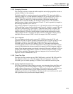
2-133. Oscillator Amplitude Control
Since small excess phase shifts exist in all three amplifiers and the gain of the summing
amplifier cannot be made exactly one, it is impossible to generate an amplitude-stable
sinusoidal waveform from just these elements. A control circuit consisting of an error
integrator and a linear four-quadrant multiplier is used to sense the output amplitude and
stabilize it by adjusting the loop phase shift slightly.
To do this, a fourth oscillator signal is generated using U8 to invert the output of the
quadrature amplifier. The Oscillator now has four equal-amplitude signals all spaced 90º
apart. These signals are rectified and summed by CR1-CR4 and Z6 in such a way that a
dc representation of the output amplitude is created. This dc signal is summed with a -
12V reference voltage by the error integrator circuit which contains op amp U18. If there
is a magnitude difference between the rectified dc and the reference, the output of the
error integrator changes. This in turn controls the amplitude of the oscillation. This is
done via multiplier U16, a linear-variable resistance with a value inversely proportional
to the error integrator output voltage.
If the control input (x input) to the multiplier is zero, the equivalent resistance from the
signal input (y input) is infinite. If the control input is negative, the equivalent resistance
is negative. The Y signal input of the multiplier is the quadrature amplifier output. Any
nonzero control voltage changes the phase shift of the loop by injecting a small amount
of out-of-phase current into the summing amplifier. This negative feedback is used to
stabilize the amplitude of the oscillating signal by allowing one output amplitude only to
satisfy the required conditions of oscillation. During operation in the 100 Hz range,
control line LFCOMP* and comparator U20A turn off FET Q6.
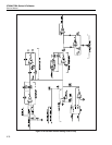
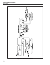
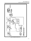
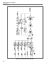
2-134. Phase
−
locked Loop
The Oscillator Output assembly is phase locked to an external frequency to increase
frequency accuracy. This external frequency comes from the High-Resolution Oscillator
on the Current/Hi-Res assembly (A7) or from an external source connected to the rear-
panel PHASE LOCK IN jack.
The frequency capture range is approximately ±5% of the nominal output frequency
range. This is done by comparing the oscillator output frequency SUMMING AMP OUT
or INT OSC OUT against the external frequency source P LOCK HI with a phase
detector. The P LOCK HI signal is referenced to P LOCK LO. The phase-locked loop
circuit locks SUMMING AMP OUT to the external frequency when the calibrator is in
the 22V range or less. The phase-locked loop circuit locks INT OSC OUT, which is 180º
out of phase from SUMMING AMP OUT, during calibrator operation at higher voltages.
This occurs because the output from the Power Amplifier and High Voltage assemblies
(which are used to generate the higher voltage ranges) are 180º out of phase from the
Oscillator output. When the Calibrator is in the higher voltage ranges, control line 0/180
and op amp U31B turn on Q7, which selects INT OSC OUT to the Zero Crossing
Detector.
Since the phase detector circuit requires digital inputs, both signals are converted to
square waves using U23A/B as dual zero crossing detectors. Square waves from the zero
crossing detector circuitry are fed to the phase detector circuit containing U22A/B and
U21. The phase detector circuit looks for the falling edge of both signals. The first signal