


Theory of Operation
Digital Section Detailed Circuit Description
2
2-29
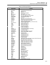
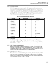
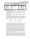
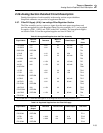
Table 2-6. Front Panel Memory Map
Name Read/Write Address
OTDCS* R/W D02000 to D027FF
DMDCS* R/W D02800 to D02FFF
ENCODERCS* R D03000 to D033FF
ENCODERRESET* W D03000 to D033FF
LED_OUTPUT_CNTRL R D03400 to D037FF
LED_LATCH_EN W D03400 to D037FF
KEYBOARDCS* R/W D03800 to D03BFF
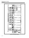
2-50. Control Display Circuitry
Control display circuitry consists of a 26-row by 256-column vacuum-fluorescent dot
matrix display under the control of PLD U4, four high voltage grid drivers (U20-U23),
four high voltage anode drivers (U16-U19), a filament switching circuit, and 1K x 8 (1
KB) dual-port RAM U1.
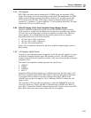
This display is divided into 129 grids; alternate grids contain two anode columns lettered
B C or D A. Grid G129 and column C in grid G128 are not used. Each column contains
26 individual anodes.
IC U4 is an EP900 Programmable Logic Device (PLD). It provides the timing and
control signals for control display circuitry. Display data written by the microprocessor
into the Control Display’s dual port RAM (U1) is read by U4 and sent serially to the high
voltage anode drivers. Both the anode and grid drivers are serial TTL-level input, 32-bit
parallel high voltage output devices. IC U4 also controls the grid timing and display
refresh.
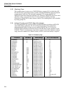
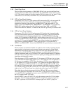
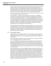
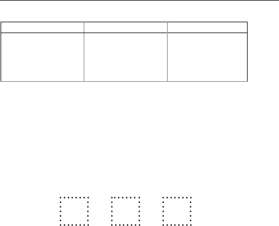
B C D A B C
G4 G5 G6
Adjacent columns in adjacent grids are driven, while the opposite columns are turned
off. For instance, grid G4 contains columns B and C, and grid G5 contains columns D
and A. G4 and G5 are driven simultaneously while anode columns G4-C and G5-D are
activated, and G4-B and G5-A are driven off. Next, grids G5 and G6 are driven
simultaneously, while columns G5-A and G6-B are activated, and G5-D and G6-C are
driven off. This pattern is repeated for all 128 grids at a refresh rate of about 75 Hz.
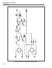
This particular scheme was selected because of the way the anode drivers are loaded
with display data. Both the A and C (U16 and U18), and B and D (U17 and U19) anode
drivers’ input registers are latched with the same data, while the output drivers are
appropriately enabled and displaying the data previously strobed to the driver outputs
from the input registers. The input register data is strobed to the output drivers while all
of the drivers are disabled, or blanked. Following this, either the A and B drivers are
enabled to display the A-B data, when the C and D drivers, latched with A-B data, are
disabled, or the C and D drivers are enabled to display the C-D data, when the A and B
drivers, latched with C-D data, are disabled.
Control display filament driver circuitry consists of transistors Q1 through Q6 and zener
diodes VR1 and VR2, with associated resistors. The transistors are driven by 7406 open
collector drivers U13B and U13A. These drivers are controlled by AOUT and BOUT.
AOUT and BOUT are synchronous, non-overlapping, three-eighths duty cycle, 57.6 kHz
timing signals generated by U3. Each signal is alternately active high for 6.51 us, with a
dead time between active signals of about 2.17 us to allow for turn-off times of the drive