


Theory of Operation
Analog Section Detailed Circuit Description
2
2-135
• Seven control lines which comprise the CONTROL BUS
• A low-level 3.6864 MHz clock (CLOCK, CLOCK*)
• Eight data lines RPD0-RPD7
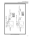
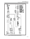
Interfacing between the Rear Panel data bus (D100-D107) and the CPU data bus (RPD0-
RPD7) is done with a bus transceiver U1.
2-215. Wideband AC Module (Option -03)
The Option -03 Wideband AC Module consists of the Wideband Oscillator assembly
(A6) and the Wideband Output assembly (A5).
The wideband module operates in conjunction with the Oscillator Output assembly
(A13), and provides calibrated output voltages in the range of 300 µV to 3.5V rms at
frequencies of 10 Hz to 30 MHz, into a 50Ω load resistance. The output impedance of
the assembly is 50Ω. It is designed to drive 50Ω loads. The output of this option
connects to the Type "N" wideband connector on the Calibrator front panel.
Theory of operation for the Wideband Oscillator assembly (A6) and the Wideband
Output assembly (A5) follows under separate headings.
2-216. Wideband Oscillator Assembly (A6)
The Wideband Oscillator assembly generates sine wave outputs in the range of 1.1 MHz
to 30 MHz, (with two-digit resolution) at a nominal full scale output of 700 mV rms.
The frequency source is a ECL-level square wave with a frequency range of 1.1 MHz to
30 MHz, created in the phase-locked loop and divider circuit. The amplitude of this
square wave is controlled by the WB AMPLITUDE CONTROL line, which is a DC
signal from the Wideband Output assembly, and the circuitry contained in the amplitude
control amplifier.
The resulting variable frequency and amplitude square wave is converted to sine wave
by one of the five-pole filters. This variable frequency and amplitude sine wave is routed
to the Wideband Output assembly via connector J1 and a 75Ω coaxial cable.
2-217. Wideband Oscillator Power Supplies
The +5LH, -5LH, +17S, and -17S supplies are generated on the Regulator assembly and
routed to this assembly via the motherboard.
The -5LH supply is buffered by L12 and C49, creating the -5F supply.
The +5LH supply is divided by R66 and R67 to create the +2.5 supply which is the
reference voltage for comparators in U7, U10, and U11.
Zener diode VR1 and resistor R39 create the +12 supply from the +17S supply. Zener
diodes VR4 and VR5, resistors R40 and R41, and diodes CR8 and CR9 create the -12, -
11, and -9.5 supplies from the -17S supply. These are used throughout the Wideband
Oscillator assembly.
2-218. Wideband Oscillator Digital Control
The digital control circuit on the Wideband Output assembly creates control lines WB
MUXA, WB MUXB, WB MUXC, WB FBS, and WB ON/OFF*. These lines are routed
to the Wideband Oscillator via the motherboard.
Control lines WB MUXA, WB MUXB, and WB MUXC are inverted and level-shifted
by comparators in U7 to create the control lines for multiplexer U6. They are also used
by the filter-select circuitry.