


5700A/5720A Series II Calibrator
Service Manual
2-74
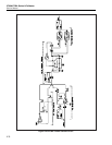
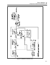
All power supplies used by this assembly are generated by the Guard Crossing/Regulator
assembly (A17) except the +5 OSC supply, which is generated by a three-terminal +5V
regulator (U25) from the +15 OSC supply. The ±15 OSC supplies are buffered by L3,
L4, C34 and C35 to create the ±15A supplies, and L1, L2, C86 and C87 to create the
±15B supplies. A +2.5V reference voltage is created from the +5LH supply by resistors
R52 and R53. A -200 mV reference voltage is created from the -15V OSC supply by
resistors R57 and R58 for use exclusively by the protection circuitry for thermal sensors
U14 and U16.
2-120. Oscillator Control Digital Control
The digital control circuit contains an 82C55 Programmable Peripheral Interface (U20)
and latching relay drivers (U23, U24). The 82C55 is controlled via the guarded digital
bus, and has three ports that generate 24 outputs. Port A (PA0-PA7) is a common input
bus (DATA) for the relay drivers (U23, U24) and the 14-bit DAC (U10). Relay driver
U23, which controls latching relays K1 through K4, K6, and K8, is strobed by PC5 and
enabled by PC7 of port C. Relay driver U24, which controls latching relays K5, K7, and
K9, is strobed by PC6 and enabled by PC7 of port C. The SW control bus contains
control lines SW1-SW4 from PB4-PB7 of port B which control a CMOS analog switch
IC U19. PC1-PC4 of port C create control lines GCAL, AC*/DC, DAC* and BIT14*
respectively. The Oscillator Output assembly (A13) generates two more control lines:
LFCOMP* and HFCOMP*. These control lines are routed to this assembly via the
motherboard and enter on pins 18A/C and 19A/C of connector P502.
A self-diagnostic circuit contains a multiplexer (U18) and resistor networks Z5 and Z6.
It monitors ±15V, VREF, and the outputs of the error integrator and 14-bit DAC. These
inputs are divided by the resistor networks, while U18 applies one to the SDL line. The
SDL line is routed to the DAC assembly (A11) to be measured by the adc circuit.
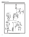
2-121. Oscillator Input Switching
Relay K1 selects an input to the Oscillator Control assembly. During ac voltage
operation, relay K1 is reset. This connects the input (SENSE HI) to the averaging
converter and the ac sense buffer to OSC SENSE HI. The reference voltage, VREF, is
connected to both DAC/OSC OUT HI and DAC/OSC SENSE HI, which is the dc
voltage from the DAC assembly (A11). During internal calibration K1 is set, so VREF is
the 6.5V reference voltage (BRF6 and BSRF6) from the DAC assembly. The input to the
averaging converter and ac sense buffer is DAC/OSC OUT HI and DAC/OSC SENSE
HI from the DAC assembly.
2-122. Sense Current Cancellation
The SENSE HI current cancellation circuit, containing op amp U1, Q1, Q2, K8, K2B and
associated components, supplies the current into SENSE HI (Z2 pin 1) so that no current
is pulled from the OSC SENSE HI line. During operation in the 2.2V and 22V, range K8
is set so the input is OSC OUT. In the 220V range K8 is reset so OSC SENSE HI is
connected to the input. Relay K2B is reset in the 2.2V range and set in the 22V range.
Transistors Q1 and Q2 form a bootstrapped supply for U1.
The SENSE LO current cancellation circuit, built around op amp U2, forces the return
current back to SCOM instead of OSC SENSE LO. Relay K2A is reset in the 2.2V range
and set in the 22V range.
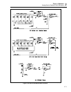
To better understand the detailed circuit descriptions for the averaging converter, error
intergrator, and three-pole filter, refer to Figure 2-19.