5700A/5720A Series II Calibrator
Service Manual
2-84
that makes a positive to negative transition causes the phase detector to turn on either the
positive (CR5, CR6) or the negative (CR7, CR8) charge pump, depending on which
signal is first. The Charge Pump is turned off when the other signal makes its transition.
Thus the signal with the highest frequency has its respective charge pump pulsed on and
off while the other charge pump remains off.
The accumulated charge is integrated by the loop filter circuit, which contains op amp
U31A, multiplexer U17, Z1, and C75-C84. Multiplexer U17 is controlled by the PLOCK
RNG control bus from the digital control circuit. This multiplexer changes the cross-over
point of the loop filter by selecting C83 and C84 for feedback in the 100 Hz range.
Capacitors C81 and C82 are used for the 1 kHz range, C79 and C80 for the 10 kHz
range, C77 and C78 for the 100 kHz range, and C75 and C76 for the 1 MHz range.
The output of the loop filter controls two multipliers (U15 and U19) similarly to the
amplitude control section. The only difference is that the signal input is derived from the
in-phase signal. In the case of U15, the input signal is QUADRATURE AMP OUT,
which changes the unity-gain frequency of the oscillator amplifier. In the case of U19,
the input signal is SUMMING AMP OUT, which changes the unity-gain frequency of
the quadrature amplifier. The new frequency of oscillation is the new unity gain
frequency of the integrators. Under phase-locked conditions, neither charge pump is
allowed to turn on because neither signal reaches the phase detector first.
2-135. 2
.
2V and 22V Range Output Amplifier
The 2.2V and 22V range output amplifier is an inverting wide-band low-distortion
amplifier that provides output signal OSC OUT HI at the OUTPUT binding posts in the
2.2V and 22V ranges. OSC OUT HI is used by the Power Amplifier and High Voltage
assemblies to generate the higher voltage ranges.
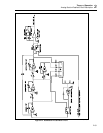
This amplifier uses a surface-mount gain block (U30) called the Oscillator Wideband
SMD PCA (A13A1) and a complementary Darlington emitter follower bootstrapped
output stage. Relay K4 selects feedback resistor R28 for the 2.2V range and R29 for the
22V range. It also changes the open-loop frequency response for each voltage range. Its
gain within a range is controlled by the gain control multiplier circuit and the dac gain
control circuit.
The dac gain control circuit contains the same 8-bit resolution resistive dac (U11) as in
the oscillator with the exception that it is controlled by the AMPL DATA control bus
from the digital control circuit. This resistive DAC provides the coarse gain control. The
gain control multiplier circuit contains a multiplier U10, which provides a small linear
control range of several dac counts. The control input to the multiplier, OSC CONT,
comes from the Oscillator Control assembly (A12). This allows the output amplitude to
be adjusted as required by the Oscillator Control Assembly. The theory of operation for
the rest of the output stage is described following the A13A1 theory.
2-136. Oscillator Wideband Smd Assembly (A13A1)
The A13A1 is a surface-mount assembly on the Oscillator Output assembly (A13) that
provides the 22V output signals of the Calibrator. It is essentially an operational
amplifier built using discrete components to provide the necessary speed, power output
and breakdown voltage required for such a high output signal.
The input stage is a differential pair (Q2 and Q3) that is buffered by a source follower
Q1. The transconductance is determined by R3, R4 and R26. The inherent input offset
voltage of this stage is corrected by U1 and U2 and related components. The output of
Q3 is level-shifted by VR5-VR7 before being applied to the mid stage. Transistor Q4
serves as a high-impedance current sink used to bias the input stage to approximately 10
mA. Potentiometer R30 adjusts the dc zero at the output of U2.


