5700A/5720A Series II Calibrator
Service Manual
2-130
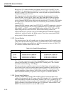
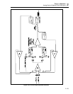
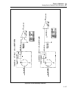
Supply voltage is applied to vco U19 whenever the Hi-Res function is used by the
circuitry containing analog CMOS switch U18A, transistor Q15, and zener diode VR3.
VCO U19 is energized when control line HI-RES ON/OFF goes low to close U18A,
which turns on transistor Q15, connecting zener diode VR3 to the -17LH power supply.
R53 and R54 divide the bias voltage input of the vco circuit to generate the HI-RES
LOOP line, which is monitored by the diagnostic circuit.
2-202. 5-500k Output Divider
The 5-500k output divider circuit contains a synthesizer IC U17 which has a reference ®
divider and a divide-by-N counter. These dividers are controlled by inputs from the
CONTROL BUS, which are latched into internal latches on the IC. Information on the
CONTROL BUS is entered and latched into U17 by NOR gate U15B and control lines
CS13* and WR*. With the phase-locked loop output frequency locked at any frequency
between 6 MHz and 12 MHz, divider U17 is programmed to divide by a value between 5
and 500,000 as required to produce the correct output frequency. The 6 MHz - 12 MHz
input from the phase-locked loop circuit is divided by the reference divider to generate
the 24 kHz-2.4 MHz frequency range at pin 18. This divided reference frequency is
connected to pin 3, which is the input of the divide-by-N-counter. The divide-by-N
counter further divides the signal to generate the 20 Hz-24 kHz frequency range at pin
15.
As an example, an output of 6.7 kHz is in range 3 with the loop locked at 6.7 MHz. (The
internal divider in U16 is programmed to divide by 6,700, resulting in 6.700 MHz.) The
two dividers in U17 are programmed for a total division of 500 (6.7 MHz/500 = 13.4
kHz). This 13.4 kHz signal is divided in half by the output switching circuit to generate
the 6.7 kHz output.
2-203. Hi-Res Output Switching
The output switching circuit contains three analog CMOS switches in U18, and flip-flops
in U21. Flip-flop U21A divides the reference divider output of U17 by two to create the
12 kHz-1.2 MHz range. Flop-flop U21B divides the divide-by-N counter output of U17
by two to create the 10 Hz-12 kHz range. Control line HI-RES RANGE and NOR gate
U15C control the analog CMOS switches U18B and U18C. These switches select the 12
kHz-1.2 MHz or the 10 Hz-12 kHz frequency range, respectively, from the flip-flops.
Control line HI-RES ON/OFF and switch U18D connect this output square-wave signal
to the P LOCK HI line when the variable phase output function is activated by the
operator.
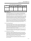
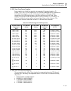
Table 2-16 shows how the dividers are set, the total division of the vco frequency, and
the vco frequency. To determine the exact vco frequency, multiply the calibrator output
frequency by the number in the total division bracket. For example, the output frequency
is set to 42 kHz and the vco frequency is 42 kHz x 200 = 8.4 MHz. Note that the total
division includes division by two by U21 in the output switching circuit.
2-204. Rear Panel Assembly (A21)
Functional circuitry on the Rear Panel assembly includes a relay control circuit, phase
lock in/variable phase out I/O circuit, address mapping, clock regeneration circuit, IEEE-
488 interface, RS-232-C interface, interfaces for the 5205A, 5215A, and 5220A
amplifiers, and a 5725A Amplifier interface. Three amplifiers can be physically
connected to the Calibrator: 5725A, 5220A with 5205A, or 5220A with 5215A. Only one
can be used at a time. Depending on the amplifier's mode of operation, the output of the
Calibrator is either an ac or a dc voltage. The following theory of operation describes
each of these circuits.


