MEMORY INTERFACING
The bus controller decodes the Inte1386
DX
microprocessor status outputs
(W/R#,
M/IO#,
and
D/C#)
and activates a command signal for the type
of
bus cycle requested.
The command signal corresponds to the bus cycle types (described in Chapter 3) as
follows:
• Memory data read and memory code read cycles generate the
EPROM
Read
Com-
mand
(EPRD#)
output.
EPRD#
commands the selected memory device to output
data.
• I/O read cycles generate the I/O Read Command
(IORD#)
output.
IORD#
com-
mands the selected
I/O device to output data.
• I/O write cycles generate the I/O Write Command
(IOWR#)
output.
IOWR#
com-
mands the selected
I/O device to receive the data on the data bus.
• Interrupt-acknowledge cycles generate the Interrupt Acknowledge
(INTA#)
output,
which
is
returned to the 8259A Interrupt Controller. The second INTAcycle com-
mands the 8259A to place the interrupt vector on the bus.
The bus controller also controls the
READY
# input to the Intel386
DX
microprocessor
that ends each bus cycle. The bus control
PLD counts wait states and returns
TIMEDLY#
after the number of wait states required
by
the accessed device. The design
of this portion of the bus controller depends on the requirements of the system; rela-
tively simple systems need less wait-state logic than more complex systems. The basic
interface described here uses a
PLD device to generate
TIMEDL
Y
#;
other designs may
use counters and/or shift registers.
6.2.7 EPROM Interface
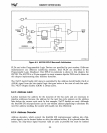
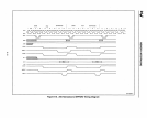
Figure
6-5
shows the signal timing for bus cycles from an Intel386
DX
microprocessor
operating at
20
MHz to a 27256 EPROM, which has a 250-nanosecond access time.
In the
EPROM
interface, the
OE#
input of each
EPROM
devices
is
connected directly
to the
EPRD#
signal from the bus controller. The wait state requirement
is
calculated
by
adding up worst-case delays and comparing the total with the Inte1386
DX
micropro-
cessor bus cycle time.
The bus cycle timings can be calculated from the waveforms in Figure
6-5.
In
the follow-
ing
example, the timings for I/O accesses are calculated for CLK2 =
40
MHz, clock
circuitry and
IOPLD1 implemented using an 85C220-66 (12 ns) PLD and IOPLD2
implemented in a 20R8 PLD. All times are in nanoseconds. Check the most recent
386'"
DX
Microprocessor Data Sheet to confirm all parameter values.
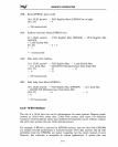
tAR: Address stable before Read
(EPRD#
fall)
(2 x CLK2
period)-
PLD RegOut Max
(ALEIO)-
Latch Enable Max
+ PLD RegOut Min
(EPRD#)
(2 x 25) -
12
-
13
+
1.5
=
26.5
nanoseconds
6-9


