


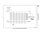
MEMORY INTERFACING
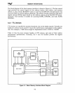
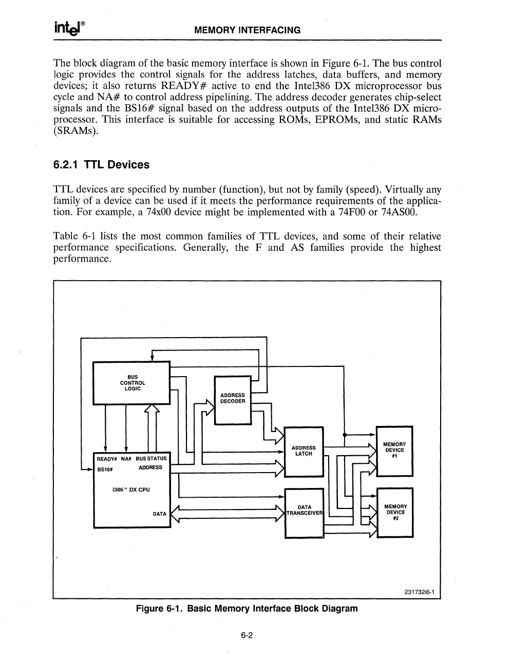
The block diagram of the basic memory interface
is
shown in Figure
6-1.
The bus control
logic provides the control signals for the address latches, data buffers, and memory
devices; it also returns READY # active to end the Intel386 DX microprocessor bus
cycle
and
NA#
to control address pipelining. The address decoder generates chip-select
signals and the
BS16# signal based on the address outputs of the Intel386 DX micro-
processor. This interface
is
suitable for accessing ROMs, EPROMs, and static RAMs
(SRAMs).
6.2.1 TTL Devices
TTL
devices are specified
by
number (function), but not
by
family (speed). Virtually
any
family of a device can be used if
it
meets the performance requirements of the applica-
tion. For example, a
74xOO
device might be implemented with a
74FOO
or
74ASOO.
Table
6-1
lists the most common families of TTL devices, and some of their relative
performance specifications. Generally, the F and
AS
families provide the highest
performance.
~
BUS
I--
CONTROL
f-
LOGIC
ADDRESS
!----
~
DECODER
flb
~
~
;I
ADDRESS
-"
MEMORY
DEVICE
LATCH
#1
READY#
NA#
BUS STATUS
"
~
---..
ADDRESS
I...-
BS16#
r-v'
'"
;386"
DXCPU
...
~
A
"\
DATA
""""-
be
MEMORY
DATA
~RANSCEIVER
'----
DEVICE
...
I'"
#2
I'"
231732i6-1
Figure 6-1. Basic Memory Interface Block Diagram
6-2