


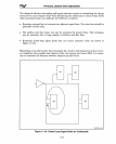

PHYSICAL DESIGN AND DEBUGGING
Room in the system should be included for the following physical features to aid
debugging:
• Two switches: one for generating the RESET signal to the Intel386
DX
microproces-
sor and one for tying the
READY#
signal high (negated).
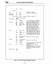
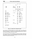
• Connections for a logic analyzer on major control signals:
Inputs to the Intel386
DX
microprocessor:
Ready
(READY#)
Next Address
(NA#)
Bus Size
16
(BS16#)
Data Bus (DO-D31)
Outputs from the Intel386
DX
microprocessor:
Address Strobe
(ADS#)
Write/Read
(W/R#),
Data/Control (D/C#),
Memory/IO (M/IO#), Lock
(LOCK#)
Address Bus (A2-A31)
Byte Enable (BEO#-BE3#)
Logic analyzer connection points should be provided to all Inte1386
DX
microproces-
sor address outputs (A2-A31 and
BEO#-BE3#)
even if there are not enough logic
analyzer inputs to accommodate all of them. Initially, only BEO#,
BE1#,
BE2#,
BE3#,
and the output of the address decoder circuit should be connected. The single
output of an address decoder circuit represents many bits of address information.
If
the address decoder does not work
as
expected, more of the logic analyzer inputs
should
be
moved to the Inte1386
DX
microprocessor address pins.
• Buffers and visual indicators (such
as
LEDs) for three or four of the critical
Inte1386
DX
microprocessor control signals. A visual indicator for the
ADS#
output,
for example, will light when the system
is
performing bus cycles.
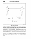
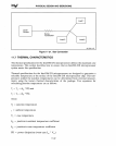
11.8.2
Bus
Interface
During initial debugging, bus-cycle operation should be simplified. The Intel386
DX
microprocessor bus interface
is
flexible enough to be tested in stages. To simplify bus
control, the initial testing should be performed with a non-pipelined address. The
NA#
input should be tied high (negated) to guarantee no address pipelining. The only signals
that need to be controlled are the
READY#
input and the BS16# input.
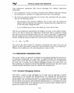
The
READY#
input on the Intel386
DX
microprocessor lets the user delay the end of
any bus cycle for as long
as
necessary. For each CLK cycle after
T2
that
READY
#
is
not
sampled active, a wait state
is
added.
READY
# can be used to provide extra time (wait
states) for slow memories
or peripherals. Wait state requirements are a function of the
device being addressed. Therefore, the address decoder must determine how many wait
states, if any, to add to each bus cycle. The address decoder circuit (usually in conjunc-
tion with a shift register) must generate the
READY#
signal when it
is
time for the bus
cycle to end.
It
is
critical for the system to generate the READY # signal; if it does not,
the Intel386
DX
microprocessor will wait forever for the bus cycle to end.
11-34