


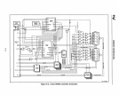
MEMORY INTERFACING
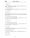
6.3.3.2 DRAM TIMING ANALYSIS
Figure
6-7
shows the signals for bus cycles from a Inte1386
DX
microprocessor to a
D RAM subsystem. This figure
will
be used for determining the worst case logic timings
for a Inte1386
DX
microprocessor operating at
20
MHz.
In this example, the timing for
DRAM
accesses are calculated for CLK2 =
40
MHz,
DRAMP2 implemented using an 85C220 (12 ns) EPLD,
DRAMPI
implemented with a
P20R8
PLD, and Refresh Address implemented with a
P20RSlO
PLD. For a registered
PLD to change states on each clock edge its maximum clock to output delay plus its
minimum setup time must be less than the time between clock edges. This
is
because the
register outputs are fed back and used as input variables in determining the PLD terms.
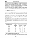
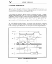
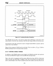
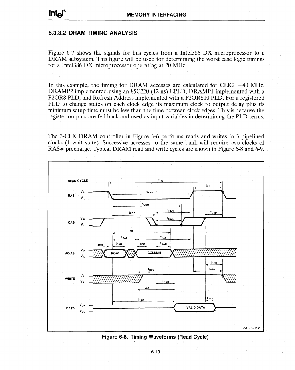
The 3-CLK DRAM controller in Figure 6-6 performs reads and writes in 3 pipelined
clocks
(1
wait state). Successive accesses to the same bank will require
two
clocks
of
RAS#
precharge. Typical
DRAM
read and write cycles are shown in Figure
6-8
and
6-9.
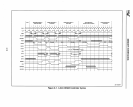
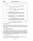
READ CYCLE
lAP
RAS
tcSH
CAS
AO·A9
~
__
~IA~A~C
________
~
________
~IO=FF~
DATA
VALID DATA
231732i6-8
Figure 6-8. Timing Waveforms (Read Cycle)
6-19