


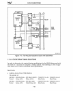


I/O INTERFACING
8.2.1 Address Decoding
Address decoding to generate chip selects must be performed whether I/O devices are
I/O-mapped or memory-mapped. The decoding technique should be simple to minimize
the amount of decoding logic.
One possible technique for decoding memory-mapped I/O addresses
is
to map the entire
I/O space of the Inte1386 DX microprocessor into a 64-kilobyte region of the memory
space. The address decoding logic can be configured so that each I/O device responds to
both a memory address and an I/O address. Such a configuration
is
compatible for both
software that uses I/O instructions and software that assumes memory-mapped I/O.
Address decoding can be simplified
by
spacing the addresses of I/O devices so that some
of the lower address lines can be omitted. For example, if devices are placed at every
fourth address, the Intel386 DX microprocessor Byte Enable outputs (BE3#-BEO#)
can be ignored for I/O accesses and each device can
be
connected directly to the same
eight data lines. The 64-kilobyte I/O space
is
large enough to allow the necessary free-
dom in allocating addresses for individual devices.
Addresses can be assigned to I/O devices arbitrarily within the I/O space or memory
space. Addresses for either I/O-mapped or memory-mapped devices should be selected
to minimize the number of address lines needed.
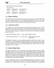
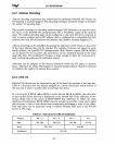
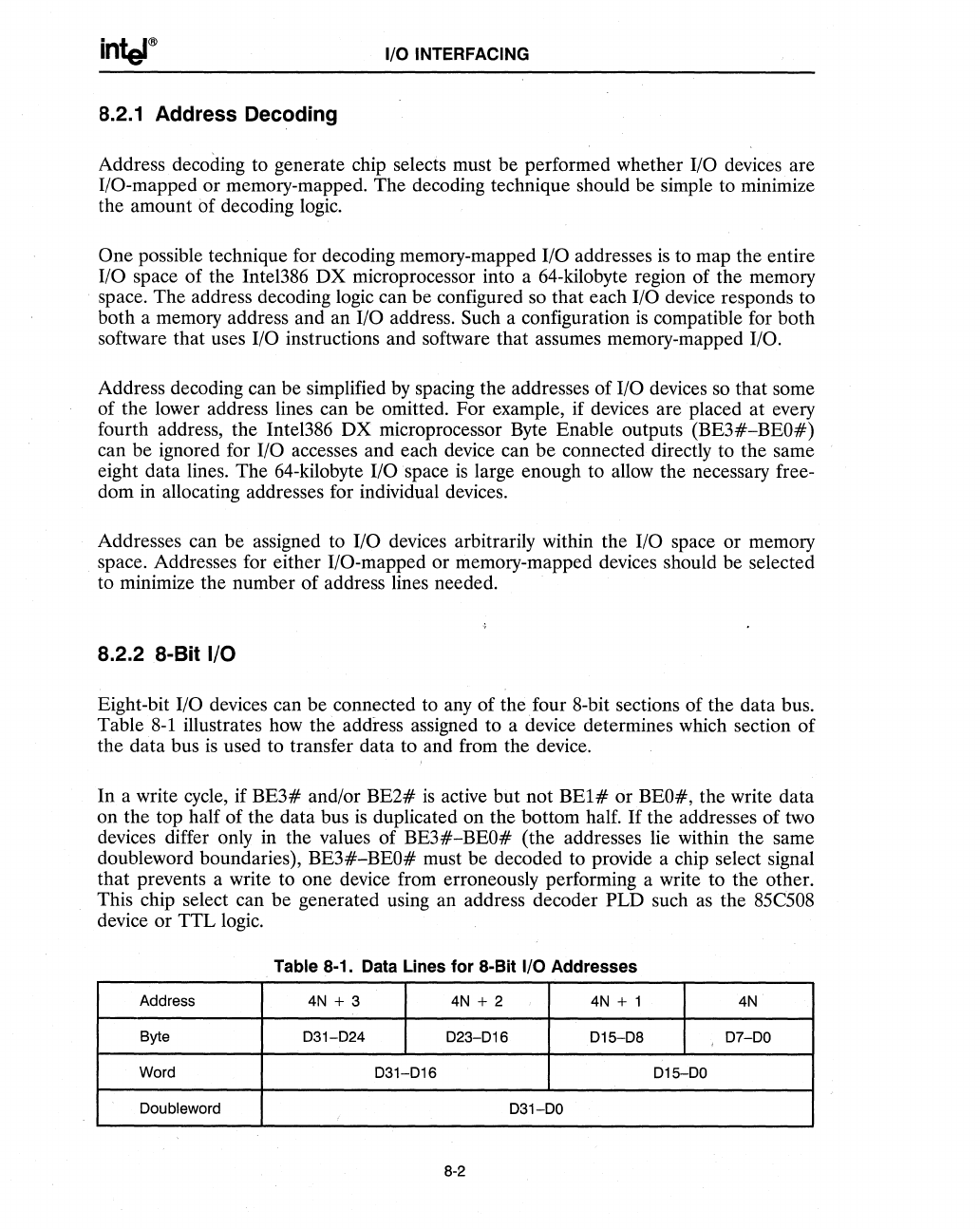
8.2.2 8-Bit I/O
Eight-bit I/O devices can be connected to
any
of the
four
8-bit sections of the data bus.
Table
8-1
illustrates how the address assigned to a device determines which section of
the data bus
is
used to transfer data to and from the device.
In
a write
cycle,
if
BE3#
and/or
BE2#
is
active but not
BEl#
or BEO#, the write data
on the top half of the data bus
is
duplicated on the bottom half.
If
the addresses of two
devices differ only in the values of BE3#-BEO# (the addresses lie within the same
doubleword boundaries), BE3#-BEO# must be decoded to provide a chip select signal
that prevents a write to one device from erroneously performing a write to the other.
This chip select can be generated using an address decoder PLD such
as
the 85C508
device or TTL logic.
Table 8-1. Data Lines for 8-Bit I/O Addresses
Address
4N
+ 3
4N
+ 2
4N
+ 1
4N
Byte
031-024
023-016
015-08
,
07-00
Word
031-016
015-00
Ooubleword
031-00
8-2