PHYSICAL DESIGN AND DEBUGGING
frequency design, including interference.
In
general, interference occurs when electrical
activity in one conductor causes transient voltage to appear in another conductor. Two
main factors increase the interference in any circuit:
1.
Variation of current and voltage ,in the lines causes frequency interference. This
interference increases with frequency.
2.
Coupling occurs when conductors are in close proximity.
Two types of interference are observed in high frequency circuits:
1.
Electromagnetic Interference (EMI)
2.
Electrostatic Interference (ESI)
.11.4.3.1 ELECTROMAGNETIC INTERFERENCE (CROSS-TALK)
Cross-talk
is
a problem
at
high operating frequencies: when operating frequency
increases, signal wavelength becomes comparable to the length of some of the intercon-
nections on .the
PC board. Cross-talk
is
a phenomenon
of
a signal in one trace which
induces another similar signal in an adjacent trace. There are two types of couplings
between parallel traces which determine the amount
of
cross-talk in a circuit. These are
called inductive coupling and radiative coupling.
Inductive coupling occurs when current in one trace produces current in a parallel trace.
This current decreases with increasing distance from the source. Hence, closely spaced
wires
or
traces will incur the greatest degree of inductive coupling. Both the traces in this
case act like normal conductors.
Radiative coupling occurs when two parallel traces act as a dipole antenna which radi-
ates signals that parallel wires can pick up. This results in the corruption of the signal
that
is
already present in the trace. The intensity of this type of coupling
is
directly
proportional to the current present in the trace. However, it
is
inversely proportional to
the distance between the radiating source and the receiver.
11.4.3.2 MINIMIZING CROSS-TALK
When laying out a board for a high frequency processor-based system, several guidelines
should be followed to minimize cross-talk.
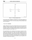
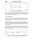
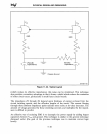
One source of cross-talk is
the
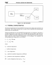
presence of a common impedance path. Figure 11-22
shows a typical layout which does not have the same earth ground and signal ground.
To reduce cross-talk, it
is
necessary to minimize the common impedance paths, which
are Z2, Z3 and Z4 shown primarily
as
ground impedances. During current switching, the
ground line voltage drops causing noise emission.
By
enlarging the ground conductor
11-25


