MEMORY INTERFACING
The
number
of
wait states for same-bank accesses applies only to back-to-back cycles
(without intervening idle bus time) to the same bank of DRAMs. Because the controller
must allow the DRAMs to precharge before starting the access, address pipelining does
not speed up the same-bank cycle; the number
of
wait states
is
identical with
or
without
address pipelining.
The
numbers in Table 6-2 are affected
by
DRAM
refresh cycles. All DRAMs require
periodic refreshing of each data cell to maintain the correct voltage levels. An access to
a memory cell, called a refresh cycle, accomplishes the refresh. During
one
of
these
periodic refresh cycles, the
DRAM
cannot respond to processor requests.
Although the distributed
DRAM
refresh cycles occur infrequently, they can delay the
current access so that the current access requires a total of up to four wait states (for the
cases marked with an asterisk
(*»
or
eight wait states (for the
other
cases).
6.3.3 DRAM Controller
The
design in this chapter
is
a 3-CLK pipelined
DRAM
controller. The timing analysis is
done
at
20
MHz.
The
design can
be
scaled to match the speed
of
your design.
Other
variations for
DRAM
control are discussed following the sample system.
6.3.3.1
3-ClK
DRAM
CONTROllER
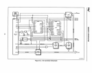
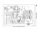
Figure
6-6
shows a schematic
of
the 3-CLK
DRAM
controller. The
DRAM
array con-
tains two banks of 32-bit-wide DRAMs. The top and bottom halves of the pictured array
represent the two banks, which
are
each divided vertically along the four bytes for each
doubleword.
The
DRAM
chips used to create
the
DRAM
banks can be
of
any length (N), and they
can
be
one, four
or
eight bits wide.
If
Nx1
DRAM
chips are used,
64
chips are required
for the two banks; if
Nx4
DRAM
chips are used,
16
chips are required; if
Nx8
DRAM
chips are used, only 8 chips are required. The banks in Figure 6-6 are made from eight
256x8
DRAM
modules,
but
another type of
DRAM
can be substituted easily.
Two Row Address Strobe (RAS) signals are generated by the controller, one for each
bank.
The
top bank
is
activated by RASO# and contains the
DRAM
memory locations
for which the Inte1386
DX
microprocessor address bit A2
is
low. The bottom bank is
activated by
RAS1#,
which corresponds to Intel386
DX
microprocessor addresses for
which A2
is
high.
Each
of
the 32
data
lines
of
the
Intel386
DX
microprocessor are connected to one
DRAM
data
bit from each bank.
If
Nx1
DRAMs are used, the corresponding data line
is
connected to both the Din and
Dout
pins.
If
Nx4
or
Nx8
DRAMs are used, each
data
line is connected only to the corresponding I/O pin.
Each bank has four Column Address Strobes
(CAS#);
one for each byte of the Intel386
DX
microprocessor
data
bus.
The
Intel386
DX
microprocessor Byte Enable Signals
(BE3#-BEO#)
map to
the
active bank's CAS signals. CASO# is generated by OR-ing
6-14


