


I/O INTERFACING
interrupt request inputs to a slave controller active. The slave controller sends an
interrupt request to the master controller, and the master controller interrupts the
Intel386 DX microprocessor. The slave controller then returns a service-routine vector
to the Intel386
DX
microprocessor. The service routine must include commands to poll
the third level of interrupt controllers to determine the source of the interrupt request.
The only additional hardware required to handle more than
64
interrupts are the extra
8259As and the chip-select logic. For maximum performance, third-level interrupt con-
trollers should be used only for noncritical, infrequently used interrupts.
8.6 80286-COMPATIBLE BUS CYCLES
Some devices (the 82258, for example) require an 80286-compatible interface in order to
communicate with the Intel386 DX microprocessor. An 80286-compatible interface must
generate the following signals:
• Address bits
Al
and
AO,
and Byte High Enable
(BHE#)
from the Inte1386
DX
microprocessor
BE3#-BEO#
outputs
• Bus
cycle
definition signals
SO#
and
SI#
from the Intel386
DX
inicroprocessor
M/IO#,
W/R#,
and
D/C#
outputs
• Address Latch Enable
(ALE#),
Dev1ce
Enable (DEN), and Data Transmit/Receive
(DT
/R
#)
signals
• I/O Read Command
(IORC#)
and I/O Write Command (IOWC#) signals for I/O
cycles
• Memory Read Command
(MRDC#)
and Memory Write Command (MWTC#)
sig-
nals for memory cycles
• Interrupt Acknowledge
(INTA#)
signal for interrupt-acknowledge cycles
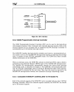
In the following example, the interface
is
constructed using the 80286-compatible
bus'
controller (82288) and bus arbiter (82289). The 82289, along with the bus arbiters of
other processing subsystems, coordinates control of the bus between the Intel386
DX
microprocessor and other bus masters. The 82288 provides the control signals to perform
bus cycles
..
Communication between the Intel386
DX
microprocessor and these devices
is
accomplished through PLDs that are programmed to perform· all necessary signal
translation and generation. Latching and buffering of the data and address buses
is
performed
by
TTL logic.
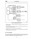
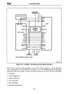
Figure 8-8 shows a block diagram of the interface, which consists of the following parts:
• AO/AI
generator-Generates
the lower address bits from Inte1386
DX
microproces-
sor BEO#-BE3# outputs
• Address
decoder-Determines
the device the Intel386
DX
microprocessor will access
• Address latches - Connect directly to Intel386
DX
microprocessor address pins
A19-A2 and the outputs of
the AO/AI generator
• Data transceivers-Connect directly to Inte1386 DX microprocessor data pins
DIS-DO
8-16