MEMORY INTERFACING
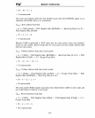
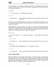
= 50 - 30 - 6 + 2
=
16
nanoseconds
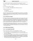
The worst case address hold time from
RAS#
occurs when the ROWSEL signal
is
at a
minimum and
RAS#
delay
is
at a maximum.
T
RAH
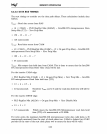
: Row address hold time
=
(1
x CLK2 period) + PLD RegOut Min (ROWSEL) + Mux Prop Min
(S
to Z) -
PLD RegOut Max
(RAS#)
=
25
+ 2 + 4 -
12
=
19
nanoseconds
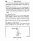
Because
CAS#
is
generated a CLK2
cycle
later for write cycles, worst case consider-
ations are the column address setup time for read cycles and the column address hold
time for write cycles.
T
ASC
: Column address setup time (read cycles)
=
(1
x CLK2) - PLD RegOut Max (ROWSEL) - Mux Prop Max
(S
to Z) + PLD
RegOut
Min (CAS#) + (2 x Or-gate Prop Min)
=
25
-
12
-
11
+
1.5
+ 6
=
9.5
nanoseconds
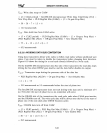
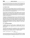
T
CAH
: Column address hold time (write cycles)
=
(2
x CLK2) - PLD RegOut Max (CAS#) -
(2X
Or-gate Prop Max) + PLD
RegOutMin (ROWSEL)
+ Mux Prop Min
(S
to Z)
= 50 - 6 - 12 + 2 + 4
=
38
nanoseconds
The write enable
(WE#)
signal
is
generated two CLK2 before
CAS#
on write
cycle
and
one CLK2 before CAS# on a read cycle.
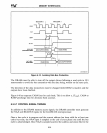
T
RCS
: Read command setup time
=
(1
x CLK2) - PLD RegOut Max
(WE#)
+ PLD RegOut Min (CAS#) + (2 x
Or-gate Prop Min)
=
25
- 6 +
1.5
+ 6
=
26.5
nanoseconds
6-21


