


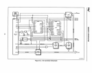
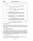
MEMORY INTERFACING
the
RAS#
from that bank and BEO# with the
CAS#
signal to enable the least-
significant byte (D7-DO). Similarly, CAS3#
is
generated
by
RAS#,
BE3#
and
CAS#
and enables the most significant byte (D31-D24).
The Write Enable
(WE#)
and the multiplexed address signals are connected to every
DRAM
module in both banks. For drive considerations the multiplexed address
is
gen-
erated separately for each bank.
A single
WE#
control signal and four CAS control signals ensure that only those
DRAM
bytes selected for a write cycle are enabled. All other data bytes maintain their
outputs in the high-impedance state. A common design error
is
to use a single
CAS#
control signal and four
WE#
control signals, using the
WE#
signals to write the
DRAM
bytes selectively in write cycles that use fewer than
32
bits. However, although the
selected bytes are written correctly, the unselected bytes are enabled for a read cycle.
These bytes output their data to the unselected bits of the data bus while the data
transceivers output data to every bit of the data bus. When two devices simultaneously
output data to the same bus, reliability problems and even permanent component dam-
age can result. Therefore, a DRAM design should use CAS signals to enable bytes for a
write cycle.
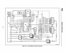
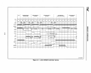
DRAMs require both the row and column addresses to be placed sequentially onto the
multiplexed address bus. A set of 74F258 multiplexers accomplishes this function.
Four 74F245 octal transceivers buffer the DRAM from the data bus. Most DRAMs used
in the 3-CLK design require these transceivers to meet the read-data float time. When a
DRAM read cycle
is
followed immediately
by
a Intel386
DX
microprocessor write cycle,
the Intel386
DX
microprocessor drives its data bus one CLK2 period after the read cycle
completes.
If
the data transceivers are omitted, the CAS inactive delay plus the
DRAM
output buffer turn-off time (t-OFF) must be less than a CLK2 period to avoid data bus
contention.
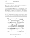
Two PLDs are used to monitor the Intel386
DX
microprocessor status signals and gen-
erate the appropriate control signals for the DRAM, multiplexer, and transceivers.
PLD
codes and pin descriptions for the 3-CLK design are listed in Appendix B of this manual.
These
PLDs, DRAMP1 and DRAMP2 contain state machines to perform the following
functions:
•
DRAMPl
Performs bus cycle tracking
Monitors the Inte1386
DX
microprocessor
DRAM
chip select logic
Signals start of
DRAM
cycles to DRAMP2
Generates the
RAS#
signals and the Address Mux select signal (ROWSEL)
Controls refresh cycle arbitration and controls the address output enables for
refresh cycles
• DRAMP2
Receives and stores DRAM refresh requests from the refresh counter
Keeps track of
DRAM
banks requiring precharge time
6-16