


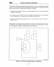

PHYSICAL DESIGN AND DEBUGGING
EPROMs, static RAMs, and peripherals all interface in much the same
way.
The
EPROM
interface
is
the simplest because EPROMs are read-only devices. RAM inter-
faces must support byte addressability during RAM write cycles. Therefore, RAM write
enables for each byte of the 32-bit data bus must be controlled separately.
The BS16# signal must be activated when the current bus cycle communicates over a
16-bit bus.
An
address decoder circuit can be used to determine if BS16# must
be
asserted during the current bus cycle.
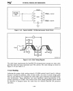
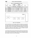
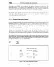
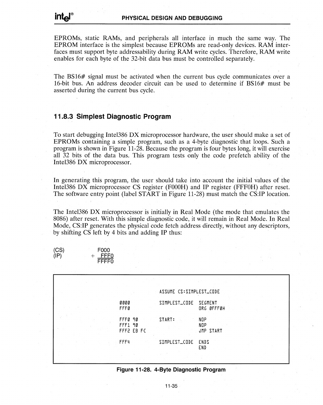
11.8.3 Simplest Diagnostic Program
To start debugging Inte1386
DX
microprocessor hardware, the user should make a set of
EPROMs containing a simple program, such
as
a 4-byte diagnostic, that loops. Such a
program
is
shown in Figure 11-28. Because the program
is
four bytes long, it
will
exercise
all 32 bits of the data bus. This program tests only the code prefetch ability of the
Inte1386
DX
microprocessor.
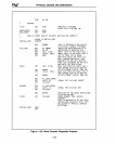
In generating this program, the user should take into account the initial values of the
Intel386
DX
microprocessor
CS
register
(FOOOR)
and IP register (FFFOR) after reset.
The software entry point (label
START
in Figure 11-28) must match the CS:IP location.
The Intel386
DX
microprocessor
is
initially in Real
Mode
(the mode that emulates the
8086) after reset. With this simple diagnostic code, it will remain in Real Mode. In Real
Mode,
CS:IP generates the physical code fetch address directly, without any descriptors,
by
shifting
CS
left
by
4 bits and adding IP thus:
(CS)
(IP)
FOOO
+
FFFO
FFFFO
ASSUME
CS:SIMPLEST_CODE
0333
SIMPLESLCODE
SEGMENT
FFF3
ORG
3FFF3H
FFF3
93
START:
NOP
FFFl
93
NOP
FFF2
EB
FC
JMP
START
FFF4
SIMPLEST_CODE
ENDS
END
Figure 11-28. 4-Byte Diagnostic Program
11-35