MEMORY INTERFACING
controller responds within
1-5
CLKs of the refresh request. The maximum latency (the
difference between the longest and shortest responses) for the design
is
therefore 5
CLKs. This time
is
spread out among all
256
accesses, so 5/256
is
subtracted in the above
equations to account for the latency period. The counter immediately resets itself after it
reaches the maximum count, regardless of this latency period.
Distributed refresh has two advantages over other types of refresh:
• Refresh cycles are spread out, guaranteeing that the Inte1386
DX
microprocessor
access
is
never delayed very long for refresh cycles. Most programs execute in approx-
imately the same time, regardless of when they are run with respect to
DRAM
refreshes.
• Distributed refresh hardware
is
typically simpler than hardware required for other
types of refresh.
6.3.5.2 BUR&T REFRESH
Burst refreshes perform all
256
row refreshes consecutively once every 4 milliseconds
rather than distributing them equally over the time period.
Once a refresh
is
performed,
the next 4-millisecond period
is
guaranteed free of refresh cycles. Time-critical sections
of code
<.:an
be executed during this time.
The 3-CLK design can be modified for burst refreshes
by
lengthening the maximum
count of the Refresh Interval Counter to cover a 4-millisecond interval and holding the
Refresh Request (RFRQ) signal active for
256
refresh cycles instead of a single refresh
cycle. The completion of
256
refresh cycles can be determined
by
clearing the Refresh
Address Counter PLD before the first refresh cycle and monitoring the outputs until
they reach the zero address again. The Row Select (ROWSEL) signal can be used to
clock the Refresh Address Counter PLD. The longer interval counter and extra logic
requires another PLD device.
6.3.5.3 DMA REFRESH USING THE 82380 DRAM REFRESH CONTROLLER
The 82380 DRAM Refresh Controller can be used to perform refresh operations. The
82380 refresh logic provides a 24-bit Refresh Address Counter. Timer 1
is
used to ini-
tiate refresh cycles. When the refresh function
is
enabled, the output of Timer
1,
TOUTl/REF#,
becomes the Refresh Request signal: The 82380 uses
DMA
operation to
perform DRAM refresh. During a DRAM refresh cycle,
TOUTl/REF#
will be acti-
vated and a Refresh Address will be placed on the Address Bus. In order to ensure that
no refresh cycles will be delayed, the Refresh Request
is
always arbitrated with the
highest priority among the DMA requests.
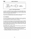
DMA refresh can be used for both 3-CLK and 2-CLK designs. To activate both
b&nks,
the 82380's Refresh Request
(TOUTl/REF#)
is
ANDed
withthe
Intel386
DX
micro-
processor's Hold Acknowledge (HLDA) to qualify for a valid refresh operation. The
output of this ANDed signal
is
connected to
theRFRQ
input of the DRAMP1 PLD (see
Figure 6-12). The DRAM State PLD must be modified to ignore chip selects. This
modification
is
needed to prevent the PLD from attempting to run a normal access cycle
after
.the refresh cycle
is
complete.
6-29


