


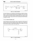
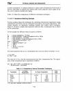

PHYSICAL DESIGN AND DEBUGGING
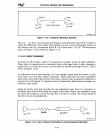
(Parasitic
C T Capacitance)
I
Chassis Ground
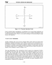
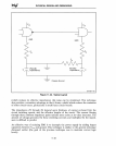
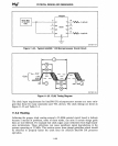
Figure 11-22. Typical Layout
Parasitic
Capacitance
J C
231732i11-22
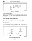
(which reduces its effective impedance), this noise can be minimized. This technique
also provides a secondary advantage in that it forms a shield which reduces the emissions
of other circuit traces, particularly in multi-layer circuit boards.
The impedances
Z2through
Z4 depend upon thickness of copper pc-board foil, the
circuit switching speeds, and the effective lengths of the traces. The current flowing
through these common impedance paths radiates more noise
as
its value increases. The
amount of voltage generated
by
these switching currents and multiplied
by
the imped-
ance
is
difficult to predict.
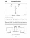
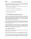
An effective
way
of reducing EMI
is
to decouple the power supply
by
adding bypass
capacitors between Vee and ground. This technique
is
similar to the general technique
discussed earlier (the goal of the previous technique was to maintain correct logic
levels).
11-26