


.
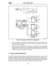
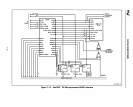
4Kx4
ADDRESS
;--
CACHE
SRAM
BANK
A
(4Kx4)
DATA
~
CSO#-
CS3#
WEN
4
4
CSO#-
OED
WEN
CS3#
;L-
ADDRESS
CACHE
SRAM
'I
BANK
B
(4K x 32)
A
DATA
'\I
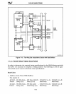
CACHE SUBSYSTEMS
01
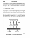
2x373
A I
_0
0
~2JA13
I--
OED
E
~t
-<I
-
-
CALEN
-"
4x245
I "
A B
"
'I
DO~D31
;!
OED
DIR
Ul
Ul
74A~~
-,--
74AS~~
-,--
"
OED
DIR
I "
A
B
"
'\I
IV
~
00-031
...
«
c
Ul
:l
mr--
<il--
0
0
~I--
!3r--
x
~-
~-
~
w
II:
c
82385
COEA#
CACHE
~~;
CWEA#
CONTROL
m
~~:
9
CSO#-CS3#
CT/R#
~
~~:
CWEB#
COEB#
;,
"'v;'
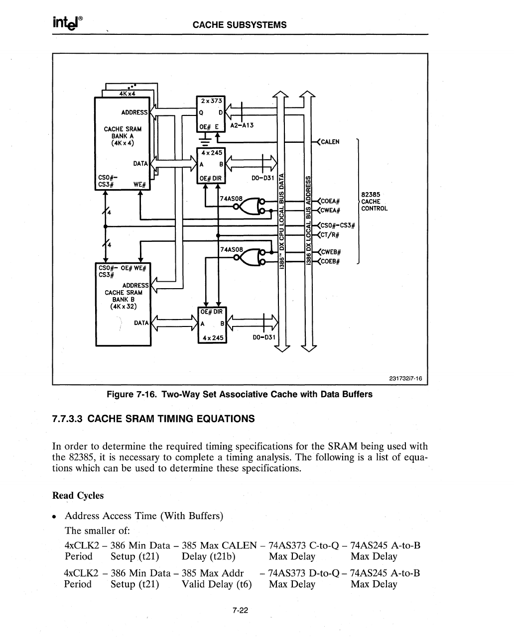
Figure 7-16. Two-Way Set Associative Cache with Data Buffers
7.7.3.3 CACHE SRAM TIMING EQUATIONS
231732i7-16
In
order to determine the required timing specifications for the SRAM being used with
the 82385, it
is
necessary to complete a timing analysis.
The
following
is
a list
of
equa-
tions which can
be
used to determine these specifications.
Read Cycles
• Address Access Time (With Buffers)
The smaller of:
4xCLK2 - 386 Min
Data
- 385 Max
CALEN
- 74AS373 C-to-Q - 74AS245 A-to-B
Period Setup (t21) Delay (t21b) Max Delay Max Delay
4xCLK2 - 386 Min
Data
- 385 Max
Addr
- 74AS373 D-to-Q - 74AS245 A-to-B
Period Setup (t21) Valid Delay (t6) Max Delay Max Delay
7-22