


PHYSICAL DESIGN AND DEBUGGING
Since the input impedance of the device
is
high compared to the characteristic line
impedance, the resistor and the line function
as
a single impedance with a magnitude
that
is·
defined
by
the value of the resistor.
When the resistor matches the line impedance, the reflection coefficient at the load
approaches zero, and no reflection will occur.
One useful approach
is
to place the ter-
mination
as
close to the loading device
as
possible.
Parallel terminated lines are used to achieve optimum circuit performance and to drive
distributed loads (an important benefit of using parallel terminations).
There are two significant advantages of using
the' parallel termination. First, it provides
an undistributed waveform along the entire line. Second, when a long line
.is
loaded in
parallel termination, it does not affect the rise and fall time or the propagation delay
of
the driving device. Note that parallel termination can also be used with wire wrap and
backplane wiring where the characteristic impedance
is
not exactly defined.
If
the
designer approximates
thy characteristic impedance, the reflection coefficient
will
be
very small. This results in minimum overshoot and ringing. Parallel termination
is
not
recommended for characteristic impedances
of
less than
100
ohms because
of
large d.c.
current requirements.
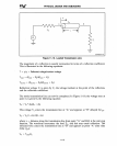
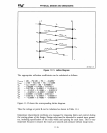
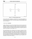
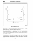
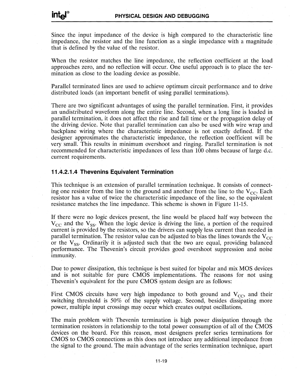
11.4.2.1.4 Thevenins Equivalent Termination
This technique
isan
extension of parallel termination technique.
It
consists of connect-
ing one resistor from
the
line to the ground and another from the line to the V cc. Each
resistor has a value of twice the characteristic impedance of the line, so the equivalent
resistance matches
the
line impedance. This scheme
is
shown in Figure
11-15.
If
there were no logic devices present, the line would be placed half way between the
V
cc
and the V ss. When the logic device
is
driving the line, a portion of the required
current
is
provided
by
the resistors, so the drivers can supply less current than needed in
parallel termination. The resistor value can be adjusted to bias the lines towards the V
cc
or the V ss. Ordinarily it
is
adjusted such that the two are equal, providing balanced
performance. The Thevenin's circuit provides good overshoot suppression and noise
immunity.
Due to power dissipation, this technique
is
best suited for bipolar and
mix
MOS devices
and
is
not suitable for pure CMOS implementations. The reasons for not using
Thevenin's equivalent for the pure
CMOS system design are
as
follows:
First
CMOS circuits have very high impedance to both ground and
Veo
and their
switching threshold
is
50% of the supply voltage. Second, besides dissipating more
power, multiple input crossings may occur which creates output oscillations.
The main problem with Thevenin termination
is
high power dissipation through the
termination resistors in relationship to the total power consumption of all of the
CMOS
devices on the board: For this reason, most designers prefer series terminations for
CMOS to CMOS connections
as
this does not introduce any additional impedance from
the signal to the ground. The main advantage of the series termination technique, apart
11-19