MEMORY INTERFACING
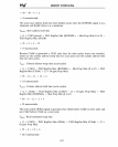
current bus
cycle
can no longer be assumed valid. The 3-clock DRAM controller does
not assert
NA#
in the first T2 but in the second T2 making it a T2p.
NA#
is
asserted at
the beginning of phase one.
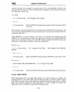
TNA
setup
=
(1
x CLK2 period) - PLD RegOut Max (CAS#)
= 25 - 6
=
19
nanoseconds The Intel386 DX microprocessor requires
NA#
setup time (T15)
to be
9
ns.
NA#
remains asserted till READY #
is
returned to the Inte1386
DX
microprocessor and
the
cycle
ends. Asserting
NA#
in the next clock
cycle
is
not necessary and only serves to
extend the hold time.
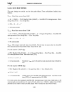
When READY #
is
asserted during a read cycle or an interrupt acknowledge cycle the
Inte1386 DX microprocessor latches the input data. During write
cycles
READY #
causes the bus cycle to terminate. The Intel386 DX microprocessor
READY#
setup and
hold times are specified in relation to the end of phase
two.
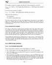
T
READY
setup:
= (2 x CLK2 period) -
(2x
And-gate Prop Max) - PLD RegOut Max (DRAM-
RDY#)
= 50 -
14
- 8
=
30
nanoseconds
Meets Inte1386 DX microprocessor READY # setup
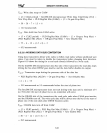
tirrte (T19)
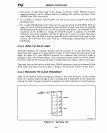
= PLD RegOut Min
(DRAMRDY#)
+
(2x
And-gate Prop Min)
=
1.5
+ 6
=
7.5
nanoseconds Meets Inte1386 DX microprocessor READY # hold time (T20)
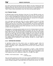
6.3.3.8 LOGIC PATHS
When performing worst case logic delay analysis, it
is
often necessary to consider the
maximum delay
of
one signal path and the minimum delay of another separate signal
path. However, when two or more signals are generated from the same device, or signal.
paths have common elements in their delay paths, it
is
more realistic to consider
the'
signal skew than to consider the theoretical maximum skew.
6-25


