MEMORY INTERFACING
Even if random accesses are made, two
DRAM
banks allow
50
percent of back-to-back
accesses to be made without waiting for the DRAMs to precharge.
The
precharge time
is
also avoided when the Intel386
DX
microprocessor has no bus accesses to be performed.
During these idle bus cycles, the most recently accessed
DRAM
bank can precharge so
that the next memory access to either bank can begin immediately.
The
DRAM
memory system design described here uses two interleaved banks of
DRAMs.
The
DRAM
controller keeps track of the precharge time for each
bank
while
allowing memory accesses to begin
as
soon
as
possible.
6.3.2 DRAM Memory Performance
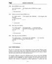
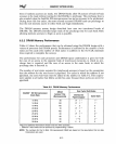
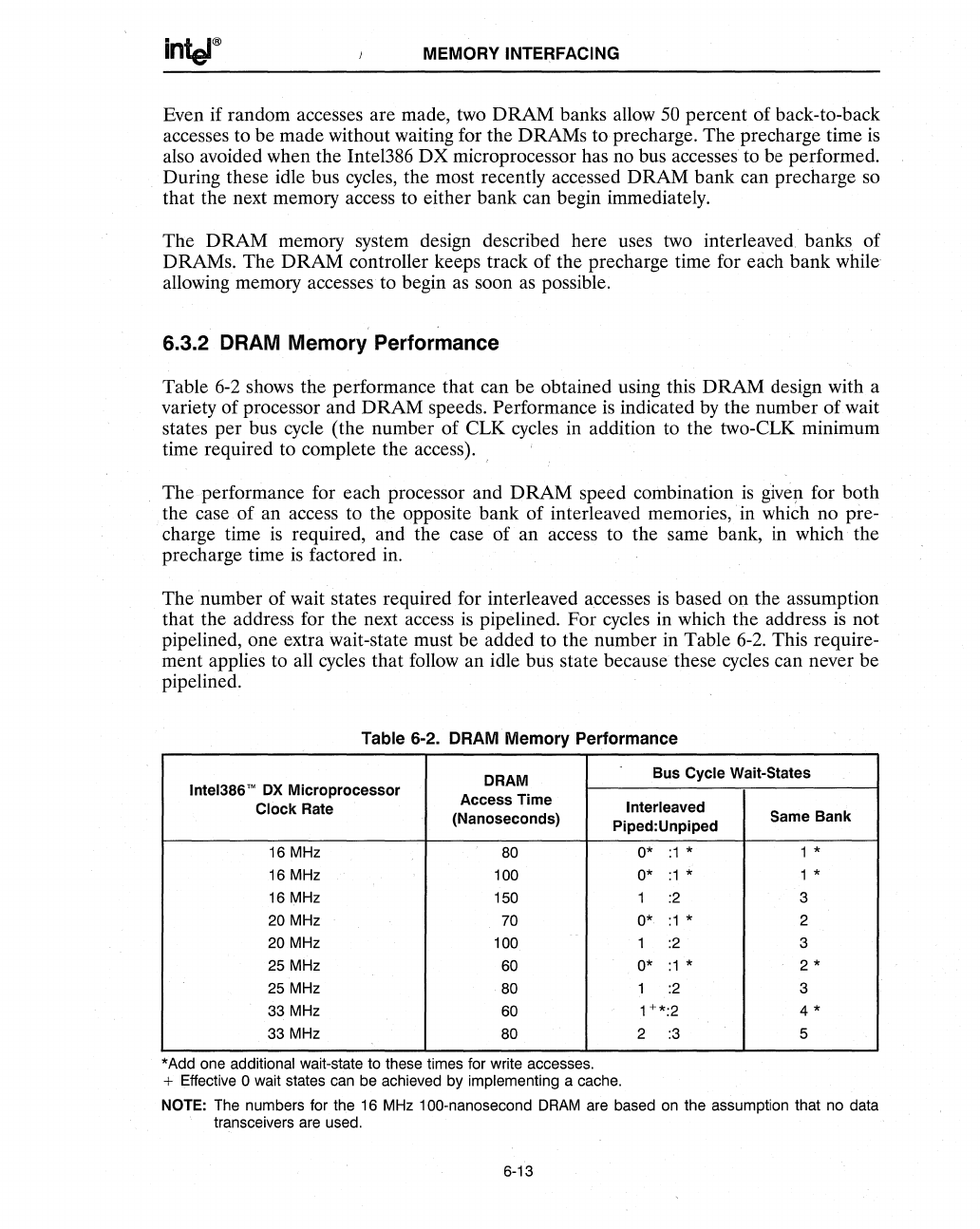
Table
6-2
shows the performance that can be obtained using this
DRAM
design with a
variety of processor and
DRAM
speeds. Performance
is
indicated
by
the number of wait
states
per
bus cycle (the number of CLK cycles in addition to the two-CLK minimum
time required to complete the access).
The performance for each processor and
DRAM
speed combination
is
given for both
the case
of
an access to the opposite bank of interleaved memories, in which no pre-
charge time
is
required, and the case of an access to the same bank, in which the
precharge time
is
factored in.
The
number of wait states required for interleaved accesses
is
based on the assumption
that the address for the next access
is
pipelined.
For
cycles in which the address
is
not
pipelined, one extra wait-state must be added to the number in Table
6-2.
This require-
ment applies to all cycles that follow an idle bus state because these cycles can never be
pipelined.
Table 6-2. DRAM Memory Performance
DRAM
Bus Cycle Wait-States
Inte1386'M
OX
Microprocessor
Access Time
Clock Rate
Interleaved
(Nanoseconds)
Piped:Unpiped
Same Bank
16
MHz
80
0*
:1
* 1 *
16
MHz
100
0*
:1
*
1 *
16
MHz 150 1
:2
3
20
MHz
70
0*
:1
* 2
20
MHz 100 1
:2
3
25
MHz
60
0*
:1
*
2 *
25
MHz
80
1
:2
3
33
MHz
60
1 +*:2
4 *
33 MHz
80
2
:3
5
*Add one additional wait-state to these times for write accesses.
+ Effective 0 wait states can be achieved by implementing a cache.
NOTE: The numbers for the
16
MHz 100-nanosecond
DRAM
are based
on
the assumption that no data
transceivers are used.
6-13


