


I/O INTERFACING
If
several I/O devices reside on the local bus,
TIMEDL
Y # logic can be simplified
by
combining into a single input the chip selects for devices that require the same number
of wait states. Adding wait states to some devices to make the wait-state requirements
of
several devices the same does not significantly impact performance.
If
the response of
the device
is
already slow (four wait states, for example), the additional wait state
amounts to a relatively small delay. Typically,
I/O devices are used infrequently enough
that the access time
is
not critical.
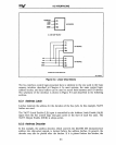
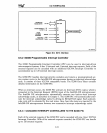
8.4 TIMING ANALYSIS FOR I/O OPERATIONS
In this section, timing requirements for devices that use the basic I/O interface are
discussed.
The
values of the various device specifications are examples only; for correct
timing analysis, always refer to the latest
data
sheet for the particular device.
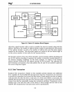
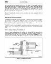
Timing for Inte1386
DX
microprocessor I/O cycles
is
identical to memory cycle timing in
most respects; in particular, timing depends on the design of the interface.
The
worst-
case timing values are calculated
by
assuming the maximum delay in the address latches,
chip select logic, and command signals, and the longest propagation delay through the
data transceivers (if used). These calculations yield the minimum possible access time
for an
I/O access for comparison with the access time
of
a particular I/O device. Wait
states must be added to the basic worst-case values until read and write cycle times
exceed minimum device access times.
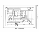
The timing requirement for the address decoder dictates that the logic be combinational
(not latched or registered) with a propagation delay less than the maximum delay calcu-
lated below .
. The CSWS signal requires a maximum decoder delay of:
(4 x CLK2)
(4 x 25)
- Intel386
DX
microprocessor Addr Valid
-
30
=
55
nanoseconds
(CLK2
=
40
MHz)
- PLD setup
-
15
The
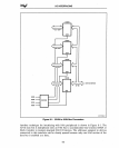
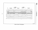
timings of the other signals can
be
calculated from the waveforms in Figure 8-5. In
the following example, the timings for
I/O accesses are calculated for CLK2 =
40
MHz,
85C220-66 (12 ns) EPLDs to implement
IOPLD1 and Clock circuitry, and a 20R8 PLD
to implement IOPLD2. All times are in nanoseconds.
tAR: Address stable before
Read
(IORD#
fall)
tAW: Address stable before Write
(IOWR#
fall)
(2 x CLK2)
- PLD RegOut Max - Latch Enable Max
+ PLD RegOut Min
(2 x 25)
-
12
-
13
+
1.5
26.5
nanoseconds
8-9