


LOCAL
BUS
INTERFACE
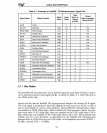
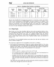
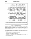
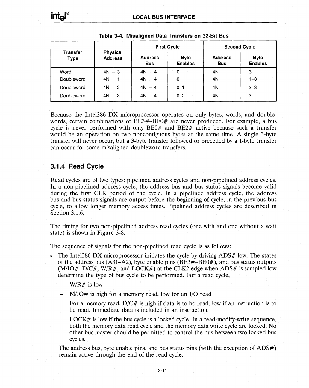
Table 3-4. Misaligned Data Transfers
on
32-Bit Bus
First Cycle Second Cycle
Transfer Physical
Type Address
Address
Byte
Address Byte
Bus Enables Bus Enables
Word
4N
+ 3
4N
+ 4
0 4N 3
Doubleword
4N + 1
4N
+ 4 0 4N
1-3
Doubleword
4N + 2
4N
+ 4
0-1
4N
2-3
Doubleword
4N + 3
4N
+ 4
0-2
4N
3
Because the Intel386
DX
microprocessor operates on only bytes, words, and double-
words, certain combinations of
BE3#-BEO#
are never produced. For example, a bus
cycle
is
never performed with· only BEO# and
BE2#
active because such a transfer
would be an operation on two noncontiguous bytes at the same time. A single 3-byte
transfer
will
never occur, but a 3-byte transfer followed
or
preceded
by
a I-byte transfer
can occur for some misaligned doubleword transfers.
3.1.4
Read
Cycle
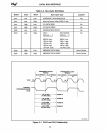
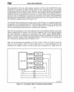
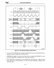
Read cycles are of two types: pipelined address cycles and non-pipelined address cycles.
In a non-pipelined address cycle, the address bus and bus status signals become valid
during the first CLK period of the cycle. In a pipelined address cycle, the address
bus and bus status signals are output before the beginning
of
cycle, in the previous bus
cycle, to allow longer memory access times. Pipelined address cycles are described in
Section 3.1.6.
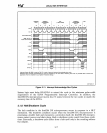
The timing for two non-pipelined address read cycles (one with and one without a wait
state)
is
shown in Figure
3-8.
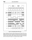
The sequence of signals for the non-pipelined read cycle
is
as
follows:
o The Intel386
DX
microprocessor initiates the cycle by driving
ADS#
low.
The
states
of
the address bus (A3I-A2), byte enable pins (BE3#-BEO#), and bus status outputs
(M/IO#,
D/C#,
W/R#,
and
LOCK#)
at the CLK2 edge when
ADS#
is
sampled
low
determine the type of bus cycle to be performed.
For
a read cycle,
W/R#
is
low
M/IO#
is
high for a memory read,
low
for an I/O read
For a memory read,
D/C#
is
high if data
is
to be read, low if an instruction
is
to
be read. Immediate data
is
included in an instruction.
LOCK#
is
low
if the bus cycle
is
a locked cycle. In a read-modify-write sequence,
both the memory data read cycle and the memory data write cycle are locked. No
other bus master should be permitted to control the bus between
two
locked bus
cycles.
The address bus, byte enable pins, and bus status pins (with the exception
of
ADS#)
remain active through the end
of
the read cycle.
3-11