


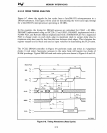
MEMORY INTERFACING
Provides the data transceiver and address latch control signals
Produces the
CAS#
and
WE#
DRAM signals
Generates the
READY#
signal to end DRAM bus cycles
A DRAM read or write access
is
requested when all the chip-select signal inputs to
DRAMPI
are sampled active simultaneously. These signals become active when all of
the following conditions exist at once:
o
M/IO#,
W/R#,
and
D/C#
outputs of the Inte1386
DX
microprocessor indicate either
a memory read, memory write, or code fetch.
o The bus
is
idle or the current bus cycle
is
ending (READY # active).
•
ADS#
is
active.
•
A31
is
low
(in this design, the lower half (two gigabytes) of the Intel386
DX
micro-
processor memory space
is
mapped to the DRAM controller).
If
DRAMPI
is
not already performing a cycle, it begins the access immediately. How-
ever, if the
DRAM
controller
is
performing a refresh cycle,
or
if it
is
waiting for the
DRAM bank to precharge, the request
is
latched and performed when the controller
is
not busy.
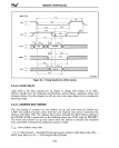
The Refresh Interval Counter
PAL
is
a timer that generates refresh requests at the
. necessary intervals. The Refresh Address Counter PLD maintains the next refresh
address. Both the Refresh Interval Counter
PLD and the Refresh Address Counter PLD
are simple enough to be replaced
by
TTL counter chips; however, the use
of
PLDs
reduces the total chip count.
If
there
is
a spare timer
or
counter in the system, it can be
used to replace one or both of these PLDs.
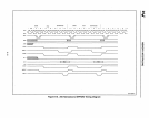
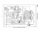
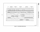
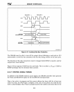
Figure
6-7
shows the timing
of
DRAM control signals for the 3-CLK design for the
following
five
sequential DRAM cycles:
1.
Read cycle
2.
Read cycle to the opposite bank (no precharge)
3.
Write cycle to that same bank (requires precharge)
4.
Refresh cycle (always requires precharge)
5.
Read cycle (cycle after refresh always requires precharge)
During a normal DRAM access, only the RAS signal that corresponds to the selected
bank
is
activated. During a refresh cycle, both RAS signals are activated. During write
cycles, only the CAS signals corresponding to the enabled bytes are activated. During
read cycles, all CAS signals are enabled.
6-17