


PHYSICAL DESIGN AND DEBUGGING
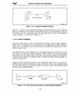
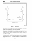
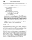
74AS244
66.67 MHz
2 18
or
50 MHz
A1
Y1
ACLK2
OSC
4
16
A2
Y2
6
Buffer
14
A3
Y3
8
12
A4
Y4
BCLK2
G
231732;11·24
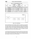
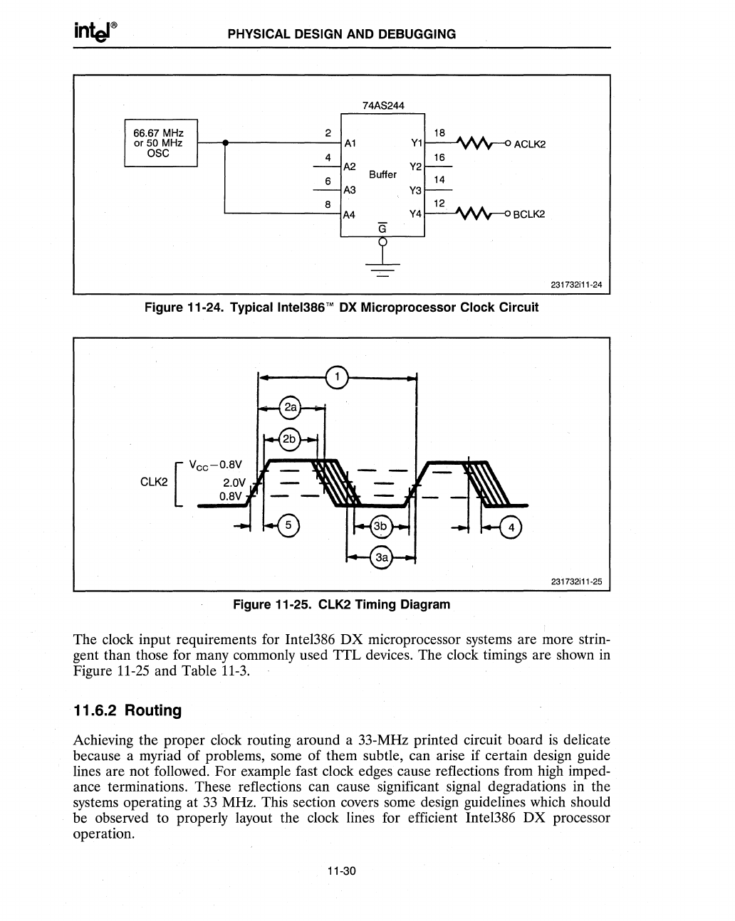
Figure 11·24. Typical Intel386™ DX Microprocessor Clock Circuit
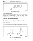
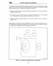
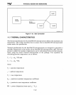
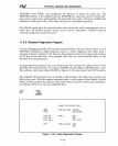
[
Vee-O.BV
CLK2
2.0V
O.BV
231732;11·25
Figure 11·25. CLK2 Timing Diagram
The clock input requirements for Intel386
DX
microprocessor systems are more strin-
gent than those for many commonly used TTL devices. The clock timings are shown in
Figure
11-25
and Table
11-3.
11.6.2 Routing
Achieving the proper clock routing around a 33-MHz printed circuit board
is
delicate
because a myriad of problems, some of them subtle, can arise if certain design guide
lines are not followed. For example fast clock edges cause reflections from high
imped-
ance terminations. These reflections can cause significant
sign.al
degradations in the
systems operating at
33
MHz. This section covers some design guidelines which should
be observed to properly layout the clock lines for efficient Intel386
DX
processor
operation.
11-30