PHYSICAL DESIGN AND DEBUGGING
GNO
5v
Ie
Packages
\.
I
~
I Oecoupling
GN0L---T-
__
+-
1
U·'~"
231732i11-2
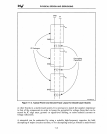
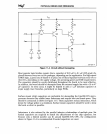
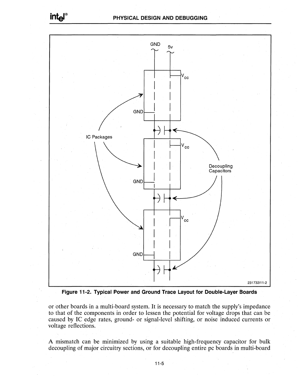
Figure 11-2. Typical Power and Ground Trace Layout for Double-Layer Boards
or other boards in a multi-board system.
It
is
necessary to match the supply's impedance
to that of the components in order to-lessen the potential for voltage drops that can be
caused
by
Ie edge rates, ground- or signal-level shifting, or noise induced currents or
voltage reflections.
A mismatch can be minimized
by
using a suitable high-frequency capacitor for bulk
decoupling of major circuitry sections,
or for decoupling entire pc boards in multi-board
11-5


