


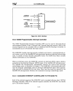
"m_l®
111'tJI
I/O
INTERFACING
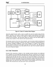
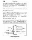
A bus interface must include enough transceivers to accommodate the device with the
most inputs and outputs on the data bus.
If
the widest device has
16
data bits and if the
I/O addresses are located
so
that all devices are connected only to the lower half of the
data bus, only two 8-bit transceivers are needed.
The
74x245
transceiver
is
controlled through two input signals:
• Data Transmit/Receive (DT /R
#)
- When high, this input enables the transceiver for
a write cycle. When
low,
it enables the transceiver for a read cycle. This signal
is
just
a latched version of the Intel386 DX microprocessor
W/R#
output.
• Data Enable
(DEN#)-When
low,
this input enables the transceiver outputs. This
signal isgenerated
by
the bus control logic.
Note that in a system using the
82380,
the data transceivers must be disabled whenever
the Intel386 DX microprocessor performs a read access to one of the internal registers
of the
82380.
Otherwise, both the
82380
and the data transceivers will be driving the
local bus which causes data contention. This can be avoided
by
decoding the
82380
address space in the bus controller logic. Together with the bus
cycle
definition signals
(W/R#, M/IO#), the data transceivers can be disabled
by
deactivating the
DEN#
signal.
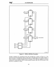
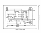
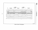
8.3.4 Bus Control Logic
The bus control logic for the basic I/O interface
is
the same
as
the logic for the memory
interface described in
Section
6.2.
The bus controller decodes the Intel386 DX micro-
processor status outputs (W/R#, MIIO#, and
D/C#)
and activates a command signal for
the
type
of
bus cycle requested. The command signal corresponds to the bus
cycle
types
(described in Chapter 3)
as
follows:
•
EPROM
data read and memory code read cycles generate the Memory Read Com-
mand
(EPRD#)
output.
EPRD#
commands the selected memory device to output
data.
• I/O read cycles generate the I/O Read Command
(IORD#)
output.
IORD#
com-
mands the selected I/O device to output data.
• I/O write cycles generate the I/O Write Command
(IOWR#)
output.
IOWR#
com-
mands
the
selected memory device to receive the data on the data bus.
Interrupt-acknowledge cycles generate the Interrupt Acknowledge
(INTA#)
output,
which
is
returned to the 8259A Interrupt Controller.
The bus controller also controls the READY # input to the Intel386
DX
microprocessor
that ends each bus
cycle.
The IOPLD2 bus control PLD counts wait states and returns
TIMEDL Y # after the number of wait states required
by
the accessed device. The design
of this portion of the bus controller depends on the requirements of the system;
rela-
tively simple systems need less wait-state logic than more complex systems. The basic
interface described here uses a PLD
device to generate T1MEDL Y
#;
other designs may
use counters and/or shift registers.
8-8