


Figure
1-1
, 1-2
2-1
2-2
3-1
3-2
3-3
3-4
3-5
3-6
3-7
3-8
3-9
3-10
3-11
3-12
3-13
3-14
3-15
3-16
3-17
3-18
3-19
3-20
3-21
5-1
5-2 r
5-3
6-1
6-2
6-3
6-4
6-5
6-6
6-7
6-8
6-9
6-10
6-11
6-12
7-1
7-2
7-3
7-4
7-5
7-6
7-7
7-8
7-9
7-10
7-11
7-12
7-13
7-14
TABLE OF CONTENTS
Figures
Title
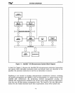
Intel386™
DX
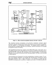
Microprocessor System Block Diagram ................................. .
Micro
Channel-Compatible Solution with
82311
Chip Set ........................... .
Instruction Pipelining ..................................................................................... .
Intel386™
DX
Microprocessor Functional Units ............................................ .
ClK2
and
ClK
Relationship .......................................................................... .
Intel386™
DX
CPU
Bus States Timing Example ...................................... : .... .
Bus
State Diagram (Does Not Include Address Pipelining) ......................... .
Non-Pipelined Address and Pipelined Address Differences ........................ .
Consecutive Bytes
in
Hardware Implementation .......................................... .
Address, Data Bus, and Byte
Enables for 32-Bit Bus ............ ; ....................
..
Misaligned Transfer ............................................... , ........................................ .
Non-Pipelined Address Read Cycles ............................................................ .
Non-Pipelined Address Write Cycles ............................................................ .
Pipelined Address Cycles .............................................................................. .
Interrupt Acknowledge Bus Cycles ............................................................... .
Internal
NA#
and
BS16#
logic
.................................................................... .
32-Bit and 16-Bit Bus
Cycle Timing .............................................................
;.
32-Bit and 16-Bit Data Addressing ................................................................ .
Using
ClK
to Determine Bus Cycle Start ..................................................... .
Clock Generator ............................................................................................. .
'ADS# Synchronizer ....................................................................................... .
Error Condition Caused by
Unlocked Cycles ............................................... .
lOCK#
Signal during Address Pipelining .................................................... .
Bus
State Diagram with HOLD State ............................................................ .
RESET,
ClK,
and
ClK2
Timing .................................................................... .
Intel386™
DX
CPU
System with Intel387'M
DX
Math Coprocessor .............. .
Pseudo-Synchronous
Interface ..................................................................... .
Software Routine to Recognize the Coprocessor ............................. : ........... .
Basic Memory
Interface Block Diagram ............................................ , ........... .
PlD
Equation arid Device Implementation ................................................... .
85C220,
EPlD
Macrocell Architecture ........................................................... .
I/O Controller Schematic ............................................................................... .
250 Nanosecond
EPROM
Timing Diagram .................................................. .
3-ClK
DRAM
Controller Schematic ........
~
...................................................... .
3-ClK
DRAM
Controller Cycles ..................................................................... .
Timing Waveforms (Read
Cycle) ...................................................... , ............ .
Timing Waveforms (Write
Cycle) ................................................................... .
Avoiding Data Bus Contention ...................................................................... .
Tap
Delay Line ............................................................................................... .
Refresh Request Generation ..................................................
, ...................... .
Cache Memory
System ................................................................................. .
Fully Associative Cache Organization ................................................ : .......... .
Direct Mapped Cache Organization .............................................
, ................ .
Two-Way
Set Associative Cache Organization ............................................. .
Stale Data Problem ........................................................................................ .
Bus Watching ................................................................................................. .
Hardware Transparency ................................................................................ .
Non-Cacheable Memory ................................................................................ .
Example of Cache Memory Organization ..................................................... .
Intel386™
DX
Microprocessor System Bus Structure ................................... .
Intel386™
DX
Microprocessor/82385 System Bus Structure ........................ .
Intel386™
DX
Microprocessor/82385 Interface ............................................. .
Direct Mapped Cache without Data Buffers .................................................. .
Direct Mapped Cache with Data Buffers ....................................................... .
xii
Page
1-2
1-3
2-1
2-3
3-4
3-5
3-6
3-7
3-8
3-9
3-10
3-12
3-14
3-15
3-17
3-19
3-20
3-21
3-25
3-26
3-27
3-31
3-32
3-34
3-36
5-3
5-5
5-7
6-2
6-5
6-6
6-8
6-10
6-15
6-18
6-19
6-20
6-24
6-27
6-30
7-1
7-4
7-5
7-7
7-9
7-10
7-11
7-12
7-15
7-16
7-17
7-18
7-20
7-21