


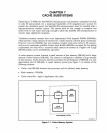
MEMORY INTERFACiNG
may
reduce overall system performance less than adding a wait state. Reducing the clock
frequency affects the time for both external bus activity
and.
internal computations. The
relationship between clock frequency and system performance
is
approximately linear.
Table
4-2
gives relative performance versus wait states and operating frequency.
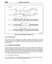
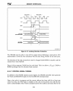
6.3.5 Refresh Cycles
All
DRAMs require periodic refreshing of their data. For most DRAMs, periodic acti-
vation of each of the row
a~dress
signals internally refreshes the data in every column of
the
row.
Almost all DRAMs allow a RAS-only refresh cycle, the timing of which
is
the
same
as
a read cycle, except that only the RAS signals are activated (no
CAS
signals),
. and all of the data pins are in the high impedance state.
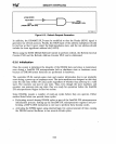
The 3-CLK design uses RAS-only refresh. The address multiplexer
is
placed in the high
impedance state, and the Refresh Address Counter
PLD
is
enabled to output the
address of the next row to be refreshed. Then the
DRAMP1 PLD activates both RASO#
and RAS1# to refresh the selected
row
for both banks at once. After the refresh
cycle
is
complete, the Refresh Address Counter PLD increments so that the next refresh
cycle
refreshes the next sequential row.
The frequency of refreshing and the number of rows to be refreshed depend on the type
of DRAM. For most larger DRAMs (64KxN and larger), only the lower eight multi-
plexed address bits
(A7-AO,
256
rows) must be supplied for the refresh cycle; the upper
address bits are ignored. The Refresh Address Counter
PLD must output only eight bits
and only the lower eight bits of the address multiplexer must be placed in the high
impedance state. The
OE#
signals of the higher order address multiplexers can be tied
low.
Larger DRAMs generally require refresh every 4 milliseconds. The following sec-
tions describe refresh specifically for larger DRAMs, although the concepts apply to
smaller DRAMs.
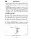
6.3.5.1 DISTRIBUTED REFRESH
In distributed refresh, the
256
refresh cycles are distributed equally within the
4-millisecond interval. Every 15.625 microseconds (4 milliseconds/256), a single row
refresh
is
performed. After 4 milliseconds all
256
rows have been refreshed, and the
pattern repeats.
The Refresh Interval Counter
PLD
is
programmed to request a single distributed
refresh
cycle
at intervals slightly under
15.625
microseconds. The counter requests a new
refresh
cycle
after a preset number of CLK cycles. This number
is
dependent on the
CLK frequency and can be calculated
as
follows for a 20-MHz CLK signal:
20
MHz x
15.625
microseconds -
5/256
= 312.48
i = 312 CLK cycles
The term 5/256
is
subtracted to allow for the time it
takestheDRAMPl
PLD to respond
to the request. Refresh requests are
always
given highest priority; however, if a DRAM
access
is
already in progress, it must finish before the refresh
cycle
can start. The 3-CLK
6-28