9-30 SA-1100
Developer’s Manual
System Control Module
Also, the SA-1100 provides the power manager scratchpad register (PSPR) for saving any general
processor state during sleep. This register may be written by the processor and the contents will
survive sleep mode. The bits in this register are not explicitly used by the SA-1100, but may be
used by software to index into ROM space to retrieve memory controller configuration, for
example.
Note: The nRESET pin must not be asserted during sleep mode if the DRAM contents are to be
preserved. The assertion and subsequent negation of nRESET during sleep mode causes the
SA-1100 to clear the FS bit in the force sleep register, assert PWR_EN, time the PLL lock
sequence, and subsequently negate the internal reset signal. This causes the SA-1100 to perform a
normal boot sequence because all information about the previous sleep state is lost.
9.5.3.7 Reviving the DRAMs from Self-Refresh Mode
Because the DRAMs are placed in self refresh prior to the sleep mode shutdown, their contents are
preserved during sleep. After exiting sleep, software must reconfigure the DRAM control registers,
which lost power during sleep mode, and then take the DRAMs out of self-refresh mode. Clearing
the DRAM hold (DH) bit in the power management status register (PMSR) will cause the
RAS<3:0> and CAS<3:0> pins to return to the negated state (high) in preparation for a DRAM
access.
9.5.4 Notes on Power Supply Sequencing
On the SA-1100, as on the SA-110, it is important that VDDX (3.3 V nominal) power-up occur
before VDDI (1.5 V nominal). One approach to ensuring this sequencing is to power the 1.5-V
supply using the 3.3-V supply. On the SA-1100, a second simple option is available. If the
PWR_EN output is used to enable the 1.5-V supply, the SA-1100 will enforce the required
sequencing by holding PWR_EN deasserted until the 3.3-V supply is sufficiently high.
9.5.5 Assumed Behavior of an SA-1100 System in Sleep Mode
The assumed model of an SA-1100 system in sleep mode is one in which the system is relatively
quiet. In particular, there should be no gratuitous switching on of the SA-1100 input pins. Although
there will be some switching in GPIOs to bring the processor out of sleep and potentially on the
VDD_FAULT and BATT_FAULT pins, the switching is a low-frequency activity and usually
brings the SA-1100 out of sleep mode.
The major concern is for power dissipation in sleep and requirements for the power supplies on the
processor during sleep. The SA-1100 generates these supplies using several on-chip regulators with
limited current capacity. Excessive activity on-chip pins might load these regulators beyond their
capacity and result in droop of the on-chip supplies. One example is that of a component tied to one
of the GPIO pins that constantly transmits to the processor. If the system design indicated that
activity from this detector should not bring the SA-1100 out of sleep, the transitions from this
GPIO might result in switching in the processor that would exceed the sleep current limit. This
concern exists regardless of whether the GPIO is enabled as a wake-up source.
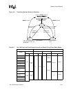
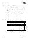
Figure 9-3 shows the three power-related modes of the SA-1100 and the actions that cause
transitions between the modes. Table 9-2 summarizes what power and clock supplies are used by
each module within the SA-1100, as well as the status of the power and clock supplies to each unit
during each of the three power-related modes.


