SA-1100 Developer’s Manual 11-179
Peripheral Control Module
11.12.10.6 External Clock Select (ECS)
The external clock select (ECS) bit selects whether the on-chip 3.6864-MHz clock is used by the
SSP or if an off-chip clock is supplied via GPIO pin 19. When ECS=0, the SSP uses the on-chip
3.6864-MHz clock to produce a range of serial transmission rates ranging from 7.2 Kbps to a
maximum of 1.8432 Mbps. When ECS=1, the SSP uses GPIO<19> to input a clock supplied from
off-chip. The frequency of the off-chip clock can be any value up to 3.6864 MHz. This off-chip
clock is useful when a serial transmission rate, which is not an even multiple of 3.6864 MHz, is
required for synchronization with the target off-chip slave device. When using GPIO pin 19 for the
input clock, the user must also set bit 19 of the GPIO alternate function register (GAFR), and clear
bit 19 of the GPIO pin direction register (GPDR). See the System Control Module chapter.
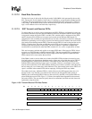
The following table shows the bit locations corresponding to the three different control bit fields
within SSP control register 1. The reset state of all bits is unknown (indicated by question marks)
and must be initialized before enabling the SSP. Note that writes to reserved bits are ignored and
reads return zero.
Address: 0h 8007 0064 SSP Control Register 1: SSCR1 Read/Write
Bit 151413121110 9 8 7 6 5 4 3 2 1 0
Reserved ECS SPH
SP
O
LBM TIE RIE
Reset0000000000??????
Bit Name Description
0RIE
Receive FIFO interrupt enable.
0 – Receive FIFO one- to two-thirds full or more condition does not generate an interrupt
(RFS bit ignored).
1 – Receive FIFO one- to two-thirds full or more condition generates an interrupt (state
of RFS sent to interrupt controller).
1TIE
Transmit FIFO interrupt enable.
0 – Transmit FIFO half-full or less condition does not generate an interrupt (TFS bit
ignored).
1 – Transmit FIFO half-full or less condition generates an interrupt (state of TFS sent to
interrupt controller).
2LBM
Loopback mode.
0 – Normal serial port operation enabled.
1 – Output of transmit serial shifter is connected to input of receive serial shifter
internally and control of TXD4, RXD4, SCLK, and SFRM pins is given to the PPC unit.
3 SPO
Serial clock polarity.
0 – The inactive or idle state of SCLK is low.
1 – The inactive or idle state of SCLK is high.
4SP
Serial clock phase.
0 – SCLK is in its inactive state one full cycle at the start of the frame and one-half cycle
at the end of the frame.
1 – SCLK is in its inactive state one-half cycle at the start of the frame and one full cycle
at the end of the frame.
5ECS
External clock select.
0 – on-chip clock used to product the SSP’s serial clock and control all timing.
1 – Clock input using GPIO pin 19 to drive the serial clock and all timing when serial
rates that are not a multiple of 3.6864 MHz are needed.
Note that bit 19 within GFAR and GPDR must be correctly configured within the system
control module.
15..6 —
Reserved.


