SA-1100 Developer’s Manual 2-7
Functional Description
2.4 Memory Map
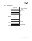
Figure 2-3 shows the SA-1100 memory map. The map is divided into four main partitions of
1 Gbyte each.
The bottom partition is dedicated to static memory devices (ROM, SRAM, and Flash) and to the
PCMCIA expansion bus area. It occupies addresses 0h0000 0000 through 0h3FFF FFFF. This
space is divided into four 128 Mbyte blocks for static memory devices and two 256 Mbyte blocks
for PCMCIA.
The static memory space is intended for ROM, SRAM, and Flash memory. The bottom partition (at
0h0000 0000) is assumed to be ROM at boot time. The width of the boot ROM is determined by
the state of the ROMSEL pin. The PCMCIA interface is divided into Socket 0 and Socket 1 space.
These partitions are further subdivided into I/O, memory and attribute space.
The next partition (0h4000 0000 to 0h7FFF FFFF) is reserved. Accessing this reserved space
results in a data abort exception.
The third partition (0h8000 0000 to 0hBFFF FFFF) contains all on-chip registers (except those
specified by the ARM
V4 architecture). This block is further subdivided into four blocks of
256 Mbyte each. They contain control registers for the major functional blocks within the
processor (MECM, SCM, PCM). The LCD and DMA controllers are separate from the rest of the
PCM and occupy the top 256 Mbyte partition.
The fourth partition (0hC000 0000 to 0hFFFF FFFF) contains DRAM memory. The bank sizes for
DRAM are fixed at 128 Mbyte each. With multiple banks implemented, there probably will be
gaps in the map that should be mapped through the memory-management unit. The next 128 Mbyte
block in this partition is mapped within the memory controller and returns zeros when read. This
function is intended to facilitate rapid cache flushing by not requiring an external memory access to
load data into the cache. This space is burstable. Writes to this space have no effect. The top
384 Mbyte of this partition is reserved. Accessing this space causes a data abort exception.


