


SA-1100 Developer’s Manual 10-7
Memory and PCMCIA Control Module
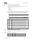
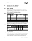
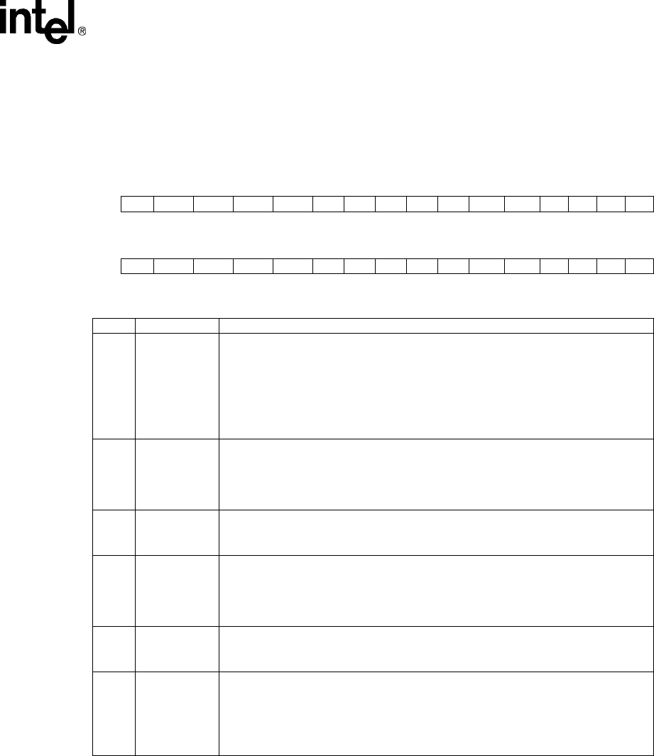
10.2.1 DRAM Configuration Register (MDCNFG)
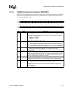
MDCNFG is a read/write register and contains control bits for configuring the DRAM. All DRAM
banks must be implemented with the same type of DRAM devices. Question marks indicate that
the values are unknown at reset.
Bit31 30 29 28 27 262524232221 2019181716
Read DRI14 DRI13 DRI12 DRI11 DRI10 DRI9 DRI8 DRI7 DRI6 DRI5 DRI4 DRI3 DRI2 DRI1 DRI0 TDL1
Reset? ? ? ? ? ?????? ?????
-?
Bit15 14 13 12 11 109 8 7 6 5 4 3210
Read TDL0 TRASR3 TRASR2 TRASR1 TRASR0 TRP3 TRP2 TRP1 TRP0 CDB2 DRAC1 DRAC0 DE3 DE2 DE1 DE0
Reset? ? ? ? ? ?????? ?0000
Bit Name Description
3..0 DE<3:0>
DRAM enable bank 3-0.
For each DRAM bank, there is an enable bit. Reads or writes to a disabled DRAM
bank trigger a single CBR refresh cycle to all banks. When all banks are disabled,
the refresh counter is disabled.
0 – DRAM bank disabled.
1 – DRAM bank enabled.
These bits are cleared by hardware reset.
5..4 DRAC<1:0> DRAM row address bit count.
00 – 9 row address bits. (Select this for support of 9x9 and 9x8 DRAMs.)
01 – 10 row address bits. (Select this for support of 10x10, 10x9, and 10x8 DRAMs.)
10 – 11 row address bits. (Select this for support of 11x11, 11x10, 11x9, and 11x8 DRAMs.)
11 – 12 row address bits. (Select this for support of 12x10, 12x9, and 12x8 DRAMs.)
6 CDB2 Clock divide by 2.
0 – CAS waveform shift register (MDCAS0, 1, 2) shifted every CPU clock.
1 – CAS waveform shift register shifted every memory clock. (CPU clock divided by 2.)
10..7 TRP<3:0> RAS precharge.
Number of memory clocks nRAS deasserted before next assertion. Between any two
DRAM accesses, nRAS is high for TRP+1 or 2 memory cycles (whichever is greater).
Between a DRAM access and a refresh, both nRAS and nCAS are deasserted for
TRP+1 or 2 memory cycles (whichever is greater).
14..11 TRASR<3:0> RAS assertion during CBR.
Number of memory clocks (minus one) nRAS asserted during CAS before RAS
refresh.
16..15 TDL<1:0> Data input latch after CAS deassertion.
00 – Read data is latched coincident with the deassertion of nCAS.
01 – Read data is latched one CPU clock cycle after the deassertion of nCAS (useful for
EDOs).
10 – 2 clocks later.
11 – 3 clocks later.