SA-1100 Developer’s Manual 11-177
Peripheral Control Module
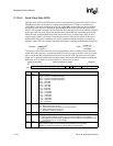
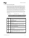
11.12.10 SSP Control Register 1
The SSP control register 1 (SSCR1) contains six different bit fields that control various functions
within the SSP.
11.12.10.1 Receive FIFO Interrupt Enable (RIE)
The receive FIFO interrupt enable (RIE) bit is used to mask or enable the receive FIFO service
request interrupt. When RIE=0, the interrupt is masked and the state of the receive FIFO service
request (RFS) bit within the SSP status register is ignored by the interrupt controller. When RIE=1,
the interrupt is enabled, and whenever RFS is set (one), an interrupt request is made to the interrupt
controller. Note that programming RIE=0 does not affect the current state of RFS or the receive
FIFO logic’s ability to set and clear RFS, it only blocks the generation of the interrupt request. Also
note that RIE does not affect generation of the receive FIFO DMA request, which is asserted
whenever RFS=1.
11.12.10.2 Transmit FIFO Interrupt Enable (TIE)
The transmit FIFO interrupt enable (TIE) bit is used to mask or enable the transmit FIFO service
request interrupt. When TIE=0, the interrupt is masked and the state of the transmit FIFO service
request (TFS) bit within the SSP status register is ignored by the interrupt controller. When TIE=1,
the interrupt is enabled, and whenever TFS is set (one), an interrupt request is made to the interrupt
controller. Note that programming TIE=0 does not affect the current state of TFS or the transmit
FIFO logic’s ability to set and clear TFS; it only blocks the generation of the interrupt request. Also
note that TIE does not affect generation of the transmit FIFO DMA request, which is asserted
whenever TFS=1.
11.12.10.3 Loopback Mode (LBM)
The loopback mode (LBM) bit is used to enable and disable the ability of the SSP transmit and
receive logic to communicate. When LBM=0, the SSP operates normally. The transmit and receive
data paths are independent and communicate via their respective pins. When LBM=1, the output of
the transmit serial shifter is directly connected to the input of the receive serial shifter internally
and control of the TXD4, RXD4, SCLK, and SFRM pins are given to the peripheral pin control
(PPC) unit.
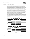
11.12.10.4 Serial Clock Polarity (SPO)
The serial clock polarity (SPO) bit selects the polarity or active/inactive state of the serial clock
(SCLK) pin when Motorola* SPI format is selected (FRF=00). When SPO=0, the inactive or idle
state of SCLK is low. Thus when the SSP is not actively transmitting/receiving data, the SCLK pin
is held low. When SPO=1, the inactive or idle state of SCLK is high. Thus when the SSP is not
actively transmitting/receiving data, the SCLK pin is held high. The programming of SPO alone
does not determine which SCLK edges are used to drive and latch data to or from the transmit and
receive pins. The programming of SPO and the serial clock phase (SPH) bit determines this. Note
that SPO is ignored in all other modes except Motorola* SPI format (FRF=00).


