10-14 SA-1100
Developer’s Manual
Memory and PCMCIA Control Module
10.3 Dynamic Interface Operation
This section describes the dynamic memory interface.
10.3.1 DRAM Overview
The dynamic memory interface supports up to four banks of identical size and type dynamic
memory on a 32-bit bus. Initialization software must set up the memory interface configuration
registers with the DRAM size, type, number of row address bits, nCAS waveforms, and timing
parameters. The SA-1100 generates accesses of 1–8 words.
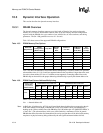
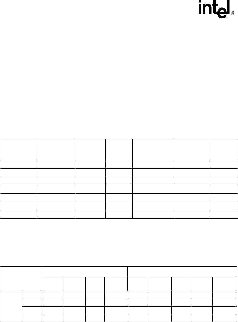
Table 10-5 shows some of the supported DRAM configurations.
Table 10-6 shows the DRAM row and column address multiplexing. For each row address size specified,
column address sizes of 11, 10, 9, and 8 are supported wherever the row address is larger than or the same
size as the column address (12 rows x 11 columns are not supported). Connecting address lines to the
DRAM chips as shown allows the proper addressing without having to specify the column address size.
.
DRAx = SA-1100 DRAM interface address pin, A(21:10) = DRA(11:0)
IAx = Internal address bit
Note: At RAS time, all address pins, A(25:0), are driven with the internal address that corresponds to the pin
of the same number. For example, a DRAM with 13 bits of row address can be accommodated by
hooking up the 13th row address line of the DRAM to SA-1100 address pin A22. (MDCNFG:DRAC is
a "don’t care".) The column address, in this case, will be limited to a maximum of 8 bits. In general,
DRAMs that utilize fewer than 8 column address bits can be used, but there will be holes in the memory
map due to no physical memory being addressed by the still significant internal address bit IA9.
Table 10-5. DRAM Memory Size Options
Bank Size
(Mbyte/Bank)
DRAM
Configuration
(Words x Bits)
Chip Size
Number
Chips /
Bank
Row bits x
Col. Bits
Max Memory
(4 Banks,
32-bit Bus)
Total
Number
of Chips
1 Mbyte 256 K x 16 4 Mbit 2 9 x 9 4 Mbyte 8
2 Mbyte 512 K x 8 4 Mbit 4 10 x 9 8 Mbyte 16
2 Mbyte 512 K x 32 16Mbit 1 10 x 9 8 Mbyte 4
4 Mbyte 1 M x 4 4 Mbit 8 10 x 10 16 Mbyte 32
4 Mbyte 1 M x 16 16 Mbit 2 10 x 10, 12 x 8 16 Mbyte 8
8 Mbyte 2 M x 8 16 Mbit 4 11 x 10, 12 x 9 32 Mbyte 16
16 Mbyte 4 M x 16 64 Mbit 2 12 x 10 64 Mbyte 8
Table 10-6. DRAM Row/Column Address Multiplexing
Number of Row
Address Bits
(as specified in
MDCNFG:DRAC)
DRAM Address Pins at RAS Time DRAM Address Pins at CAS Time
DRA11 DRA10 DRA9 DRA8-0 DRA11 DRA10 DRA9 DRA8 DRA7-0
DRAM:
12 bits IA21 IA20 IA19 IA18-10 x x IA23 IA22 IA9-2
11 bits x IA20 IA19 IA18-10 x IA23 IA22 IA21 IA9-2
10 bits x x IA19 IA18-10 x x IA21 IA20 IA9-2
9 bits x x x IA18-10 x x x IA19 IA9-2


