


SA-1100 Developer’s Manual 10-23
Memory and PCMCIA Control Module
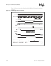
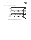
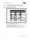
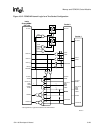
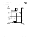
In Figure 10-9, some of the parameters are defined as follows:
tAS = Address setup to nCS = 1 CPU cycle
tCES = nCS, nCAS setup to nWE = 2 memory clock cycles (4 CPU cycles)
tASW = Address setup to nWE low (asserted) = 1/2 memory cycle (1 CPU cycle)
[For A<25:5>, tASW=5 CPU cycles. For A<4:2>, tASW=1 CPU cycle for subsequent beats in a
burst]
tDSWH = Write data setup to nWE high (deasserted) = 1/2 memory cycle + (RDN+1) memory cycles
tDH = Data hold after nWE high (deasserted) = 1/2 memory cycle (1 CPU cycle)
tCEH = nCS, nCAS held asserted after nWE deasserted = 1 memory clock cycle (2 CPU cycles)
tAH = Address hold after nWE deasserted = 1/2 memory cycle (1 CPU cycle)
nWE high time between burst beats = 1 memory cycle (2 CPU cycles)
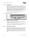
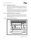
10.4.5 FLASH EPROM Interface Overview
The SA-1100 provides an SRAM-like interface for access of Flash EPROM. The RDF fields in the
MSCx registers are the latency for a read access. The RDN field controls the nWE low time during
a write cycle. RRR is the time from nCS deassertion after a read to the start of a read from a
different memory or after a write to another memory access. A single DRAM CBR refresh cycle
may be inserted between words of a burst read from Flash memory. During the refresh cycle, nCS
and nOE will be deasserted.
There are some requirements for writes to Flash memory. Flash memory space must be uncacheable
and unbuffered. Writes must be exactly the width of the populated Flash devices on the data bus (no
byte writes to a 32-bit bus or word writes to a 16-bit bus, and so on). Software is responsible for
partitioning commands and data, and writing them out to Flash in the appropriate sequence.