SA-1100 Developer’s Manual 9-5
System Control Module
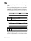
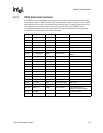
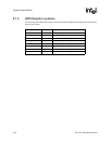
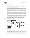
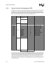
9.1.1.3 GPIO Pin Output Set Register (GPSR) and Pin Output Clear Register
(GPCR)
When a port is configured as an output, the user controls the state of the pin by writing to either the
GPIO pin output set register (GPSR) or the GPIO pin output clear register (GPCR). An output pin
is set by writing a one to its corresponding bit within the GPSR. To clear an output pin, a one is
written to the corresponding bit within the GPCR. These are write-only registers. Reads return
unpredictable values. Writing a zero to any of the GPSR or GPCR bits has no effect. Writing a one
to a GPSR or GPCR bit corresponding to a pin that is configured as an input has no effect. For
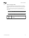
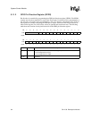
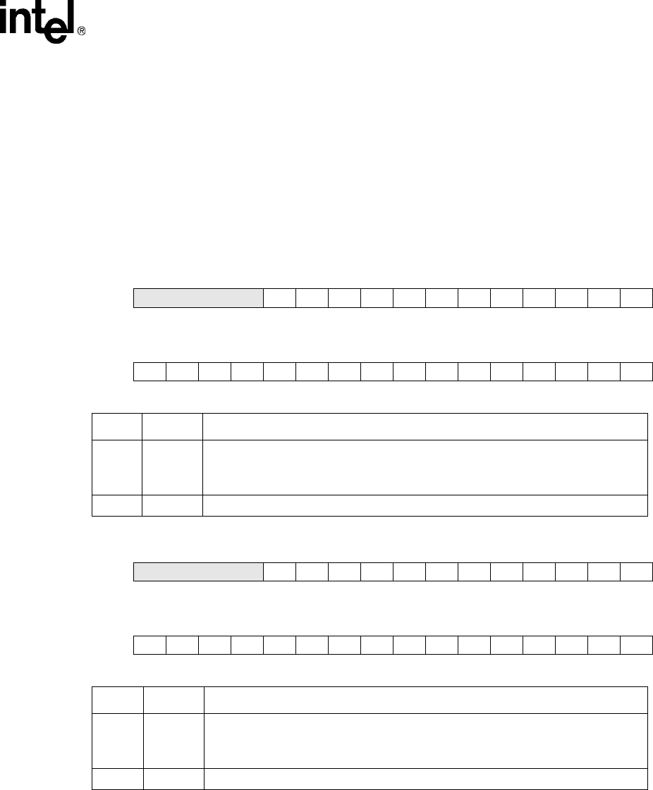
reserved bits, writes are ignored. The following tables show the locations of the GPSR bits and the
locations of the GPCR bits. These are write-only registers and reset values do not apply.
The user can test a bit within the GPLR corresponding to a pin that is configured as an output after
having set or cleared the pin state to determine if there is an external conflict on the pin. For
example, if an off-chip device is driving a GPIO output pin high and the user has cleared the pin’s
state by writing a one to its GPCR bit, the user can read the GPLR, then compare the written value
(zero) to the actual value (one) to detect the conflict.
Bit31302928272625242322212019181716
Write Reserved PS27 PS26 PS25 PS24 PS23 PS22 PS21 PS20 PS19 PS18 PS17 PS16
Reset----------------
-
Bit1514131211109876543210
Write PS15 PS14 PS13 PS12 PS11 PS10 PS9 PS8 PS7 PS6 PS5 PS4 PS3 PS2 PS1 PS0
Reset----------------
Bit Name Description
{n} PS{n}
GPIO output pin set n (where n = 0 through 27).
0 – Pin level unaffected.
1 – If pin configured as an output, set pin level high (one).
31..28 — Reserved.
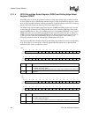
Bit31302928272625242322212019181716
Write Reserved PC27 PC26 PC25 PC24 PC23 PC22 PC21 PC20 PC19 PC18 PC17 PC16
Reset----------------
Bit1514131211109876543210
Write PC15 PC14 PC13 PC12 PC11 PC10 PC9 PC8 PC7 PC6 PC5 PC4 PC3 PC2 PC1 PC0
Reset----------------
Bit Name Description
{n} PC{n}
GPIO output pin clear n (where n = 0 through 27).
0 – Pin level unaffected.
1 – If pin configured as an output, clear pin level low (zero).
31.. 28 — Reserved.


