


11-118 SA-1100
Developer’s Manual
Peripheral Control Module
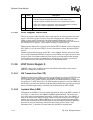
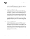
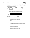
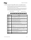
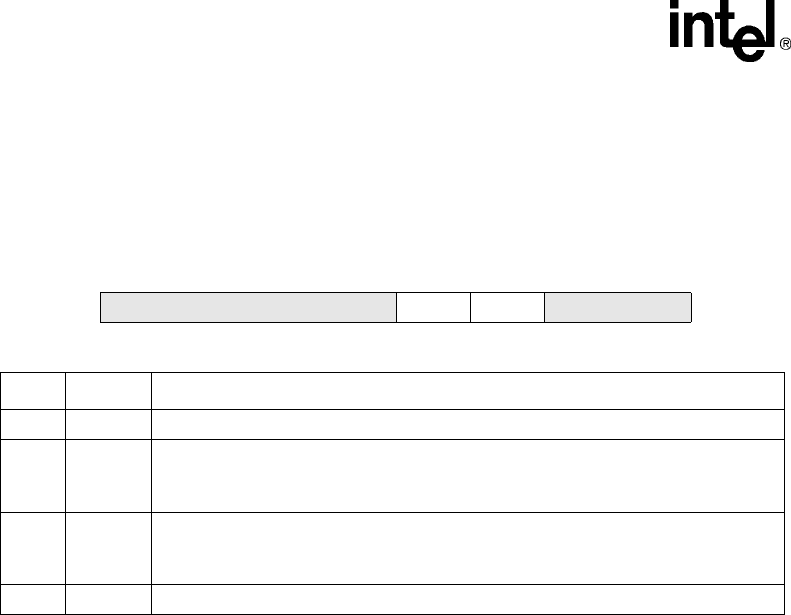
The following table shows the location of the bits within HSSP control register 2. Both bits are set
to one to ensure serial port 2’s pins default to normal “true” data operation following a reset of the
SA-1100. Note that the HSSP and UART must be disabled (RXE=TXE=0) when changing the state
of these bits. Also note that reads of reserved bits return zero and writes have no effect.
Address: 0h 9006 0028 HSCR2 Read/Write
Bit 23 22 21 20 19 18 17 16
Reserved RXP TXP Reserved
Reset 0 0 0 0 1 1 0 0
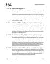
Bit Name Description
17..16 —
Reserved.
18 TXP
Transmit pin polarity select.
0 – Data output from the HSSP, UART, or PPC is first inverted before being output to TXD2.
1 – Data output from the HSSP, UART, or PPC to TXD2 is true or non-inverted data.
19 RXP
Receive pin polarity select.
0 – Data input from RXD2 is first inverted before being used by the HSSP, UART, or PPC.
1 – Data input from RXD2 to the HSSP, UART, or PPC is true or non-inverted data.
23..20 —
Reserved.