13-4 SA-1100
Developer’s Manual
AC Parameters
13.6 Timing Parameters
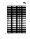
Table 13-2 lists the ac timing parameters for the SA-1100 for AA and BA parts. For timing
parameters for 2.0-V devices, contact the Intel Massachusetts Customer Technology Center.
Table 13-2. SA-1100 AC Timing Table for AA and BA Parts
Pin Name Symbol Parameter Min Max Unit Note
Memory Bus
D>31:0>
Tdfov
Memory clock fall to D<31:0> driven valid
—10 ns —
Tds
D<31:0> valid to memory clock rise/fall
0—ns 1
Tdh
Memory clock rise/fall to data invalid (input
4—ns 1
nPOE, nPWE, nPIOR,
nPIOW, PSKTSEL,
nPREG, nPCE<1,2>,
A<25:0>
Tmfov Memory clock fall to output driven valid — 10 ns
5
—
—
—
—
nIOIS16
Tio16s
nIOIS16 valid to memory clock rise (input
1—ns 6
Tio16h
Memory clock rise to nIOIS16 negated
3—ns 6
nWE, nOE Tmrov Memory clock rise to output driven valid — 10 ns
—
—
nRAS<3:0> Tmrdv
Memory clock rise to output driven valid
—12 ns —
nCAS<3:0> Tcasd
Memory clock rise/fall to nCAS<3:0> driven
—12 ns 2
nCS<3:0> Tcsd
Memory clock rise to nCS<3:0> driven valid
—10 ns —
MCP (CODEC) Interface
SFRM_C Tsfrmv SCLK_C rise to SFRM_C driven valid — 21 ns —
RXD_C
Trxds RXD_C valid to SCLK_C fall (input setup) 0 — ns —
Trxdh SCLK_C fall to RXD_C invalid (input hold) 4 — ns —
TXD_C Ttxdv SCLK_C rise to TXD_C valid — 22 ns —
LCD Controller
L_LDD<7:0> Tpclkdv L_PCLK rise/fall to L_LDD<7:0> driven valid — 14 ns 3
L_LCLK Tpclklv L_PCLK fall to L_LCLK driven valid — 14 ns 4
L_FCLK Tpclkfv L_PCLK fall to L_LFCLK driven valid — 14 ns 4
L_BIAS
Tpclkbv
L_PCLK rise to L_BIAS driven valid
—14 ns 4
All output signals Output pin transition between 0.4V and 2.4V 1.6 4.5 ns
NOTES:
1. These input pins may be sampled on either the rising or falling edge of the memory clock.
2. These output pins may be driven on either the rising or falling edge of the memory clock.
3. The LCD data pins can be programmed to be driven on either the rising or falling edge of the pixel clock
(L_PCLK).
4. These LCD signals can, at times, transition when L_PCLK is not clocking (between frames). At this time,
they are clocked with the internal version of the pixel clock before it is driven out onto the L_PCLK pin.
5. These signals are PCMCIA outputs and are driven by a state machine clocked by BCLK. The user defines
BCLK by programming the number of processor clocks per BCLK. Two processor clocks make one
memory clock cycle. To ensure proper operation, the user must adhere to the protocol description.
6. These signals are PCMCIA inputs and are sampled by a state machine clocked by BCLK. The user defines
BCLK by programming the number of processor clocks per BCLK. Two processor clocks make one
memory clock cycle. To ensure proper operation, the user must adhere to the protocol description.


